Optical device module

a technology of optical devices and modules, applied in the field of optical device modules, can solve the problems of low accuracy of lens positioning with respect damage to solid-state image sensors, signal processors and the like, and difficulty in uniform thickness of bonding agents, etc., to achieve convenient formation, high tolerance for shock, and reliable positioning

Inactive Publication Date: 2006-10-05
SHARP KK
View PDF2 Cites 38 Cited by
  • Summary
  • Abstract
  • Description
  • Claims
  • Application Information

AI Technical Summary

Benefits of technology

[0009] According to the camera module described in Japanese Patent Application Laid-Open No. 2004-297282, since the holder holding the lens is bonded to the package, when distortion occurs due to warpage, flexure or the like on the plane of the package serving as the reference plane for bonding because of the manufacturing nonuniformity of the package, the accuracy of the positioning of the lens with respect to the solid-state image sensor is decreased.
[0035] According to the present invention, when the optical path delimiter is fixed to the image sensing unit, the holder is out of contact with the sealing portion made of the resin and is in contact only with the transparent lid. There is no possibility that the positions of the holder and the transparent lid are shifted by the holder being in contact with the sealing portion, and the holder can be reliably positioned with respect to the transparent lid, so that the accuracy of the positioning of the lens with respect to the solid-state image sensor is not decreased.

Problems solved by technology

However, according to the image sensor module package described in Japanese Patent Application Laid-Open No. 2003-110946, since the holder holding the lens is fixed to the housing bonded onto the circuit board, the accuracy of the positioning of the lens with respect to the solid-state image sensor is low because of the manufacturing nonuniformity of the circuit board and the manufacturing nonuniformity of the housing.
However, since the signal processor, the solid-state image sensor and the transparent lid are placed one on another on the board and the lens holder is further bonded to the transparent lid, there is a possibility that the solid-state image sensor, the signal processor and the like are damaged due to a shock given to the lens holder.
When the bonding agent is applied, it is difficult to make the thickness of the bonding agent uniform, and there is a possibility that excess bonding agent extends to obstruct the optical path because of an error of the thickness of the bonding agent.

Method used


Image

  • Optical device module
  • Optical device module
  • Optical device module

Examples


Embodiment Construction

[0042] Hereinafter, the present invention will be concretely described with reference to the drawings showing an embodiment thereof.

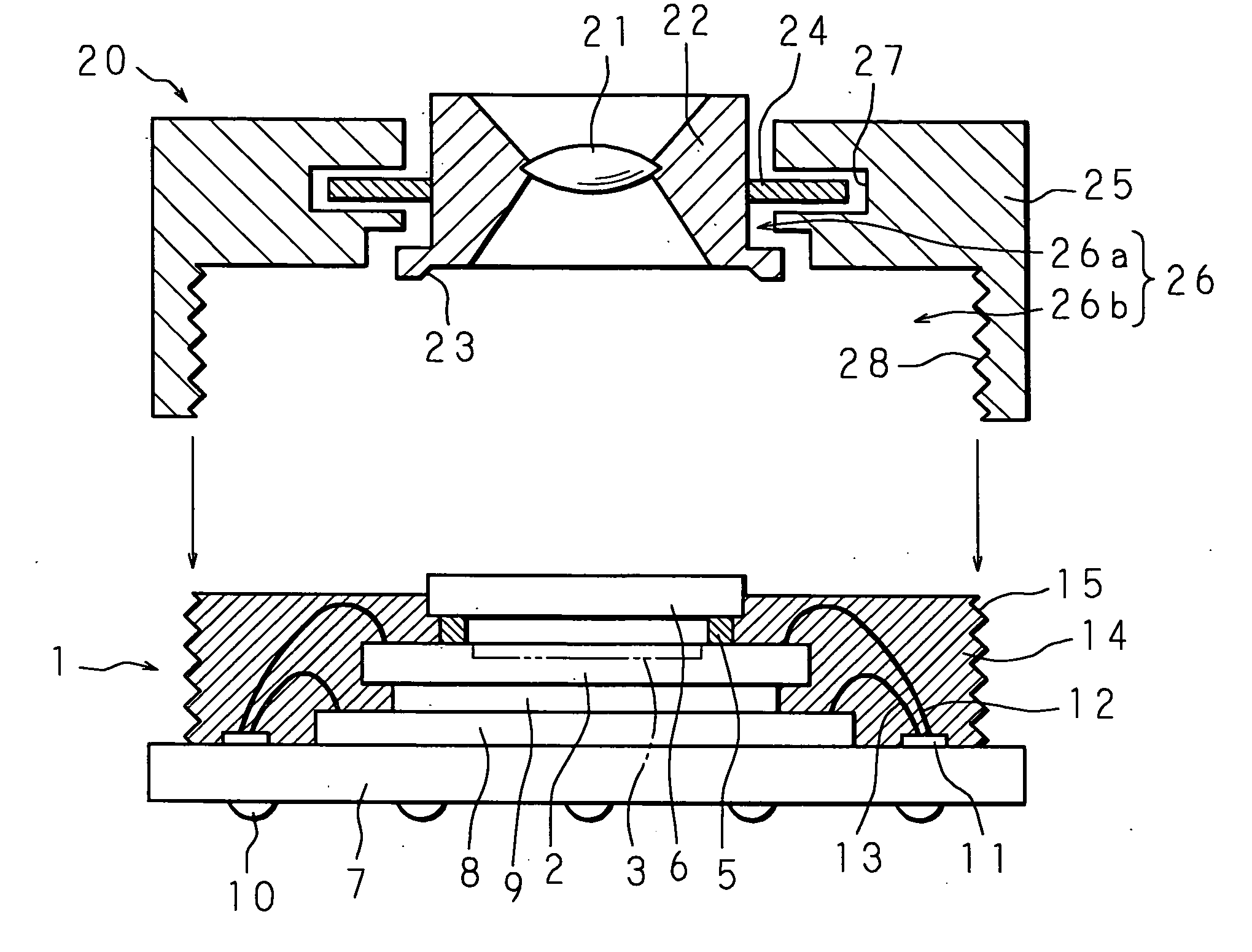
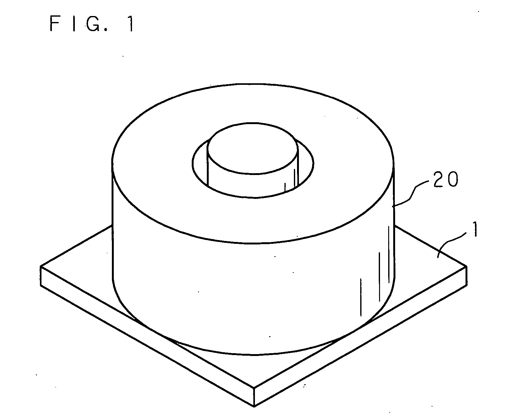
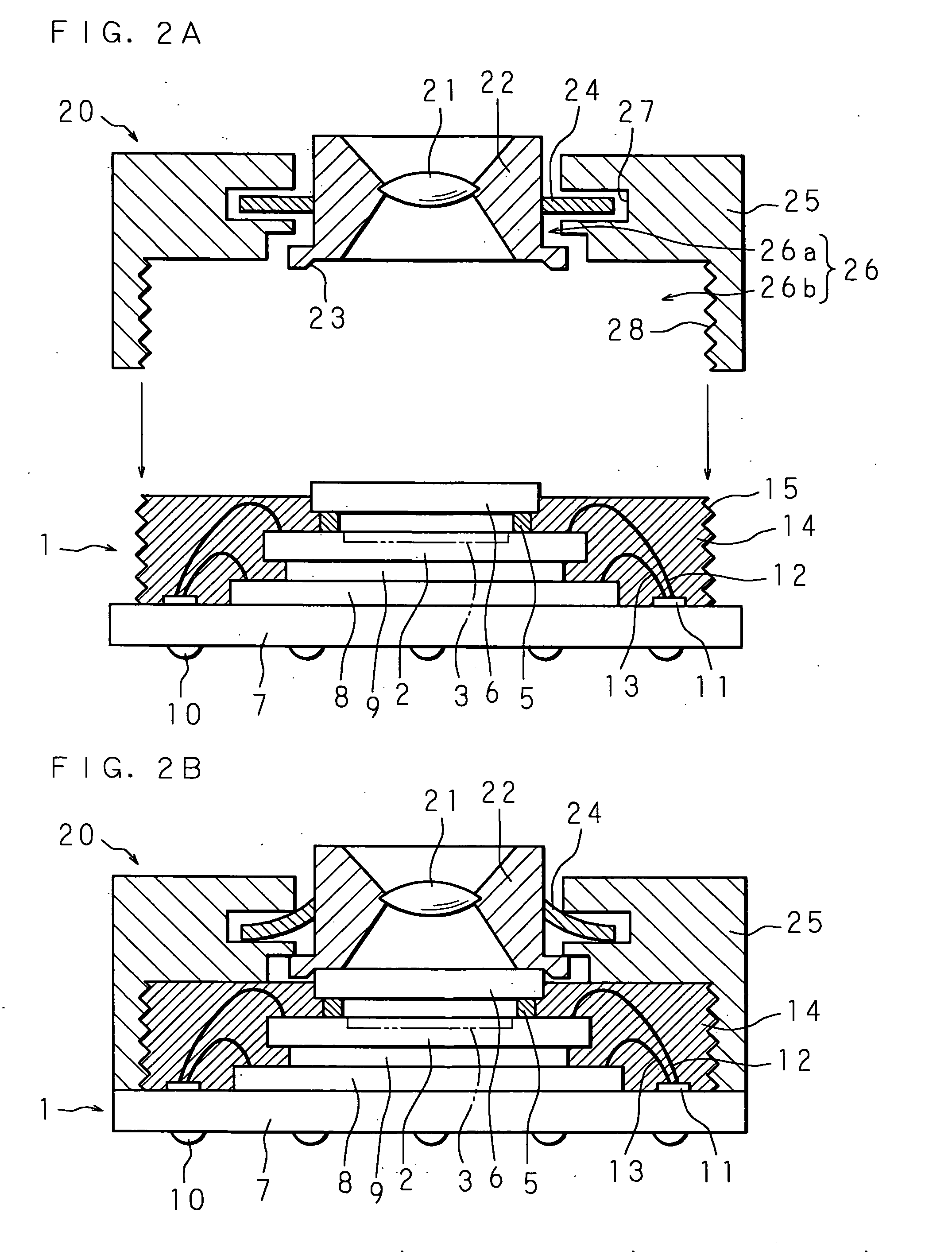
[0043]FIG. 1 is a perspective view showing the appearance of an optical device module according to the present invention. FIGS. 2A and 2B are schematic cross-sectional views showing the structure of the optical device module according to the present invention. FIG. 3 is a plan view showing the appearance of the optical device module according to the present invention. FIG. 4 is a plan view showing a solid-state image sensor of the optical device module according to the present invention. FIG. 2A shows a condition in which an optical path delimiter is not fixed to an image sensing unit of the optical device module. FIG. 2B shows a condition in which the optical path delimiter is fixed.

[0044] In these figures, reference numeral 1 represents an image sensing unit having a solid-state image sensor 2 that receives external light, and reference numeral 20 r...


PUM


Abstract

A screw portion is provided on an image sensing unit, a screw hole portion to be engaged with the screw portion is provided on an optical path delimiter, and the screw portion and the screw hole portion are engaged together to thereby fix the image sensing unit and the optical path delimiter so that a lens barrel of the optical path delimiter is in contact with a transparent lid bonded to a surface of a solid-state image sensor. The solid-state image sensor, the transparent lid, a DSP, a wiring board and the like are sealed by a sealing portion made of a resin. Even when distortion occurs due to warpage, flexure or the like on the board where the solid-state image sensor is disposed, the accuracy of the positioning of the lens with respect to a pixel area of the solid-state image sensor is never decreased, it can be prevented that the solid-state image sensor or a signal processor is damaged by an external shock, and the optical device module is easily fabricated.

Description

CROSS-REFERENCE TO RELATED APPLICATIONS [0001] This Nonprovisional application claims priority under 35 U.S.C.§119(a) on Patent Application No. 2005-103775 filed in Japan on Mar. 31, 2005, the entire contents of which are hereby incorporated by reference. BACKGROUND OF THE INVENTION [0002] The present invention relates to an optical device module incorporated in digital cameras, camera phones and the like and having a solid-state image sensor for photographing a subject, and a method of fabricating the optical device module. [0003] A solid-state image sensor provided in digital cameras, camera phones and the like is for capturing the subject to be photographed. The solid-state image sensor is integrated into a module together with a lens, an infrared intercepting material and a signal processor processing the image information captured by the image sensor, and is provided as an optical device module. In recent years, digital cameras, camera phones and the like incorporating the opti...

Claims


Application Information

Patent Timeline
Patent Type & Authority Applications(United States)
IPC IPC(8): H01J5/02G02B7/02G03B17/02H04N5/225H04N5/335
CPCH04N5/2257H04N1/024H01L2224/32145H01L2224/48091H01L2224/48227H01L2224/73265H01L2924/15311H04N23/57H01L2924/00014H01L2924/00H01L27/14H04N23/00
Inventor KINOSHITA, KAZUOHIROSUMI, NOBUHITOYASUDOME, TAKASHITSUKAMOTO, HIROAKI
Owner SHARP KK
Why Eureka
Try Eureka