
Shift register and image display apparatus containing the same

Inactive Publication Date: 2006-10-05
MITSUBISHI ELECTRIC CORP +1
View PDF7 Cites 59 Cited by
  • Summary
  • Abstract
  • Description
  • Claims
  • Application Information

AI Technical Summary

Benefits of technology

[0010] An object of the present invention is to provide a shift register capable of preventing a malfunction caused by a leakage current and an image display apparatus containing such shift register.
[0012] It is possible to control a leakage current at the first node of the shift register, which prevents the first node from dropping in voltage level while being charged. As a result, an output signal in an active state of the output terminal is ensured to follow the first clock signal, which achieves an improved operational reliability. Therefore, a display apparatus containing the shift register as a scanning-line driving circuit can achieve a normal display while preventing a malfunction.
[0014] It is possible to control a leakage current at the second node, which prevents the second node from dropping in voltage level while being charged. Accordingly, an impedance of the second transistor in an inactive state of the output terminal, that is, an output impedance of the shift register is prevented from increasing, which achieves an improved operational reliability. Therefore, a display apparatus containing the shift register as a scanning-line driving circuit can achieve a normal display while preventing a malfunction.
[0016] A leakage current, if occurred at the second node having been charged, is compensated for in an inactive state of the output terminal, which brings the second transistor into the conducting state. Accordingly, an impedance of the second transistor in an inactive state of the output terminal, that is, an output impedance of the shift register is prevented from increasing, which achieves an improved operational reliability. Therefore, a display apparatus containing the shift register as a scanning-line driving circuit can achieve a normal display while preventing a malfunction.

Problems solved by technology

Therefore, the fall time of the output signal increases, causing the output signal to be unable to follow a clock signal input to the clock terminal.
As a result, an increased fall time of the output signal in the gate-line driving circuit of a display apparatus causes a problem in that a plurality of gate lines are driven at the same time, resulting in failure to achieve a normal display (which will be described later in detail).
That is, an output impedance of the shift register increases, arising a concern that the potential at the output terminal may become unstable.
In the case where the output signal from the gate-line driving circuit thus becomes unstable, the problem of failure to achieve a normal display also arises (which will be described later in detail).

Method used


Image

  • Shift register and image display apparatus containing the same
  • Shift register and image display apparatus containing the same
  • Shift register and image display apparatus containing the same

Examples


first preferred embodiment

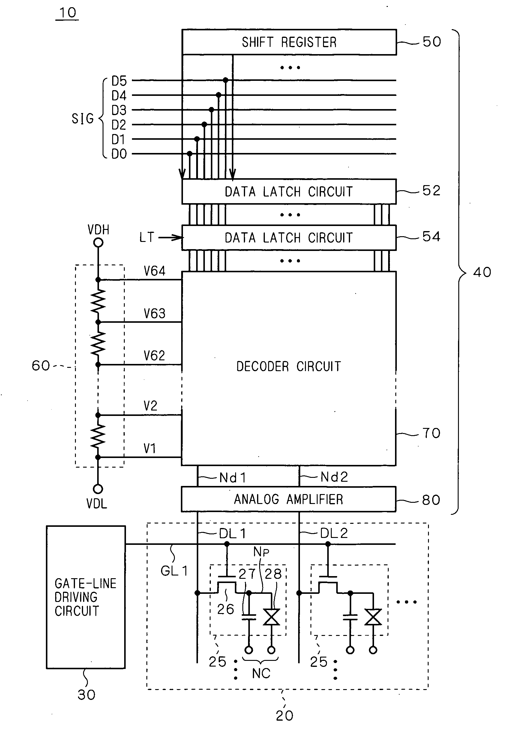
[0048]FIG. 1 is a schematic block diagram illustrating the configuration of a display apparatus according to the present invention. The overall configuration of a liquid crystal display 10 is shown as an representative example of the display apparatus.

[0049] The liquid crystal display 10 is provided with a liquid crystal array part 20, a gate-line driving circuit (scanning-line driving circuit) 30 and a source driver 40. As will be described later explicitly, a shift register according to the present embodiment is mounted on the gate-line driving circuit 30.

[0050] The liquid crystal array part 20 includes a plurality of pixels 25 arrayed in a matrix. The columns of pixels (hereinafter also referred to as “pixel lines”) are respectively provided with gate lines GL1, GL2, . . . (hereinafter also generically referred to as a “gate line GL”), and the rows of pixels (hereinafter also referred to as “pixel rows”) are respectively provided with data lines DL1, DL2, . . . (hereinafter gen...

second preferred embodiment

[0104]FIG. 9 is a circuit diagram illustrating the configuration of a unit shift register SR according to a second preferred embodiment. In the first preferred embodiment, the transistor T8 for applying the voltage VDM to the node N3 has its gate connected to the node N1, however, the transistor T8 has its gate connected to the output terminal OUT in the present embodiment. That is, the transistor T8 is turned on when the output terminal OUT transitions to VDD.

[0105] Accordingly, in the present embodiment, the voltage VDM is applied to the node N3 via the transistor T8 only between time t4 and time t5 in the timing chart shown in FIG. 4. The node N3 is kept at VDM between time t5 and time t6 as it is in the floating state in that period. More specifically, in the present embodiment, the transistor T4 is in the negative-biased state between time t4 and time t6, which prevents the occurrence of leakage current at the node N1.

[0106] A period during which the occurrence of leakage cur...

third preferred embodiment

[0109]FIG. 10 is a circuit diagram illustrating the configuration of a unit shift register SR according to a third preferred embodiment. In the present embodiment, the gate of the transistor T1 and the node N1 are connected via the transistor T9. The transistor T9 has its gate connected to a fourth power terminal s4. In the present embodiment, the fourth power terminal s4 is connected to the power source VDD, similarly to the first and second power terminals s1 and s2. Here, a connection node between the gate of the transistor T1 and the transistor T9 is defined as a node N4.

[0110] In the unit shift register SR according to the present embodiment, the node N4 is also charged to the VDD−Vth as well as the node N1 when an input signal is input to the input terminal IN. Then, the clock signal C1 input to the first clock terminal A transitions from 0V to VDD, and the node N4 rises to 2×VDD−Vth by capacitive coupling caused by the gate-to-channel capacitance of the transistor T1. Howeve...


PUM

PropertyMeasurementUnit
Electric potential / voltageaaaaaaaaaa
Semiconductor propertiesaaaaaaaaaa

Abstract

A shift register has an output stage formed by a first transistor connected between an output terminal and a first clock terminal and a second transistor connected between the output terminal and a ground. Third and fourth transistors are connected in series between the gate of the first transistor (first node) and the ground. A second node between the third and fourth transistors is connected to a power source via a fifth transistor. The fifth transistor has its gate connected to the first node. Accordingly, when the third and fourth transistors are turned off to raise the first node in level, the fifth transistor is turned on, whereby a predetermined voltage is applied to the second node.

Description

BACKGROUND OF THE INVENTION [0001] 1. Field of the Invention [0002] The present invention relates to a shift register, and more particularly, to a shift register for use as a scanning-line driving circuit for an image display apparatus or the like, which is formed by field effect transistors of the same conductivity type only. [0003] 2. Description of the Background Art [0004] An image display apparatus (hereinafter referred to as a “display apparatus”) such as a liquid crystal display includes a display panel in which a plurality of pixels are arrayed in a matrix. A gate line (scanning line) is provided for each row of pixels (pixel line), and gate lines are sequentially selected and driven in a cycle of one horizontal period of a display signal, so that a displayed image is updated. As a gate-line driving circuit (scanning-line driving circuit) for sequentially selecting and driving pixel lines, i.e., gate lines, a shift register for performing a shift operation in one frame perio...

Claims


Application Information

Patent Timeline
IPC IPC(8): G05F1/00
CPCG09G3/3677G11C19/28G11C19/184B01D39/2027B01D35/30
Inventor TOBITA, YOUICHIMURAI, HIROYUKI
Owner MITSUBISHI ELECTRIC CORP
Learn More