Supercharge Your Innovation With Domain-Expert AI Agents!

Tolerant input circuit

a technology of input buffer circuit and input voltage, which is applied in the direction of logic circuit coupling/interface arrangement, pulse technique, instruments, etc., can solve the problems of delay that cannot be avoided, pull-up operation delay of input voltage of schmitt inverter circuit, etc., to reduce the threshold value of input buffer circuit 2, prevent anomalous operation of input buffer circuit, effect of reducing hysteresis

Inactive Publication Date: 2006-10-05
SOCIONEXT INC
View PDF15 Cites 5 Cited by
  • Summary
  • Abstract
  • Description
  • Claims
  • Application Information

AI Technical Summary

Benefits of technology

[0013] In the input circuit of FIG. 1, to prevent anomalous operation of the input buffer circuit 2 when the input voltage Va decreases more than necessary, the threshold value of the input buffer circuit 2 may be lowered. However, when lowering the threshold value of the input buffer circuit 2, the rising speed or falling speed of the output signal of the input buffer circuit with respect to changes in the input voltage Va would becomes biased. More specifically, when the input voltage Va corresponding to the high level input signal is only slightly higher than the threshold value of the input buffer circuit, the rising speed of the output signal of the input buffer circuit 2 would be slower than the falling speed. This would produce a difference between the rising and falling propagation delay times of the input signal and a difference between the duties of the input and output signals. Further, when the input buffer circuit 2 is a Schmitt circuit, the lowering of the threshold value for the high level would reduce the hysteresis. This may result in an anomalous operation.
[0016] The present invention provides a tolerant input circuit that functions stably regardless of fabrication differences and without having to adjust the threshold value of the input circuit.

Problems solved by technology

This may result in an anomalous operation.
In the tolerant input circuit described in Japanese Laid-Open Patent Publication No. 2004-304475, fabrication differences in the inverter circuit and pull-up transistor may result in pull-up operation delay of the input voltage of the Schmitt inverter circuit.
However, such a delay cannot be avoided.
Further, the incorporation of the inverter circuit and the pull-up transistor enlarges the circuit scale.
Japanese Laid-Open Patent Publication No. 2000-228622 does not teach the art of compensating for a decrease in the input voltage of an inverter circuit that occurs due to fabrication differences without having to adjust the threshold value of an inverter circuit.

Method used


Image

  • Tolerant input circuit
  • Tolerant input circuit
  • Tolerant input circuit

Examples


Embodiment Construction

[0030] In the drawings, like numerals are used for like elements throughout.

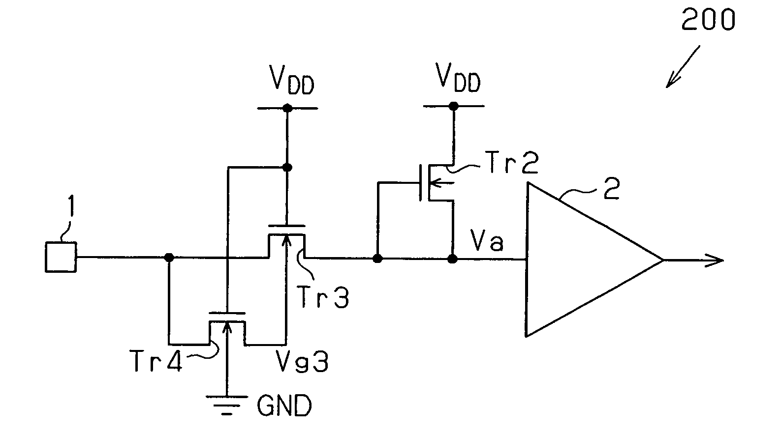
[0031]FIG. 3 is a schematic circuit diagram of a tolerant input circuit 200 according to a first embodiment of the present invention. FIG. 3 shows a transistor Tr2 and an input buffer circuit 2, which are identical to the transistor Tr2 and the input buffer circuit 2 of the prior art example shown in FIG. 1.

[0032] An N-channel MOS transistor Tr3 is connected between an input pad 1 and an input terminal of the input buffer circuit 2. The gate of the transistor Tr3 is supplied with voltage from a power supply VDD, and the transistor Tr3 functions as a step-down device. An N-channel MOS transistor Tr4 is connected between the back gate of the transistor Tr3 and the input pad 1. The gate of the transistor Tr4 is supplied with voltage from the power supply VDD. The transistor Tr4 is kept constantly activated. When the input pad 1 is provided with a voltage signal having voltage that is higher than that of the p...


PUM


Abstract

A tolerant input circuit that functions stably regardless of fabrication differences without having to adjust the threshold value of an input circuit. The tolerant input circuit includes a step-down device configured by an N-channel MOS transistor connected between an input pad and the input circuit. Voltage from a power supply is supplied to the gate of the N-channel MOS transistor in the step-down device to decrease the voltage of a high voltage signal provided to the input pad to the voltage of the power supply or lower. The signal with decreased voltage is provided to the input circuit. The tolerant input circuit includes a back gate voltage control circuit for increasing back gate voltage of the N-channel MOS transistor in the step-down device when the input pad is provided with a high voltage signal.

Description

CROSS-REFERENCE TO RELATED APPLICATIONS [0001] This application is based upon and claims the benefit of priority from the prior Japanese Patent Application No. 2005-096165, filed on Mar. 29, 2005, the entire contents of which are incorporated herein by reference. BACKGROUND OF THE INVENTION [0002] The present invention relates to a tolerant input circuit including an input terminal provided with a voltage signal having voltage that is higher than the voltage from a power supply. [0003] There may be cases when a voltage signal having voltage that is higher than the voltage from a power supply is applied to a semiconductor integrated circuit. To ensure that the semiconductor integrated circuit functions normally in such a case, the semiconductor integrated circuit incorporates a tolerant input circuit. The tolerant input circuit includes a step-down device connected between an input pad and an input terminal of an input buffer circuit. The step-down device prevents the input buffer ci...

Claims


Application Information

Patent Timeline
IPC IPC(8): H03K19/094
CPCH03K19/018507H03K19/00315H03K19/0175
Inventor SUZUKI, TOYOKITOMIDA, MITSUAKIIWAMOTO, MASAHIROUNO, OSAMU
Owner SOCIONEXT INC
Features
  • R&D
  • Intellectual Property
  • Life Sciences
  • Materials
  • Tech Scout
  • Unparalleled Data Quality
  • Higher Quality Content
  • 60% Fewer Hallucinations
Learn More