Semiconductor integrated circuit apparatus and mobile device using the same

An integrated circuit and semiconductor technology, which is applied in the field of semiconductor integrated circuit devices and mobile devices, can solve the problems that pulse signals cannot be input to the standby input terminal 51, and IC50 does not perform correct operations, etc., to achieve miniaturization, good mobility, and cost reduction Reduced effect

Inactive Publication Date: 2007-04-25
ROHM CO LTD
View PDF0 Cites 6 Cited by
  • Summary
  • Abstract
  • Description
  • Claims
  • Application Information

AI Technical Summary

Problems solved by technology

[0009] Such an IC 50 does not perform a correct operation when a pulse signal is input to the standby inpu

Method used


Image

  • Semiconductor integrated circuit apparatus and mobile device using the same
  • Semiconductor integrated circuit apparatus and mobile device using the same
  • Semiconductor integrated circuit apparatus and mobile device using the same

Examples


Embodiment Construction

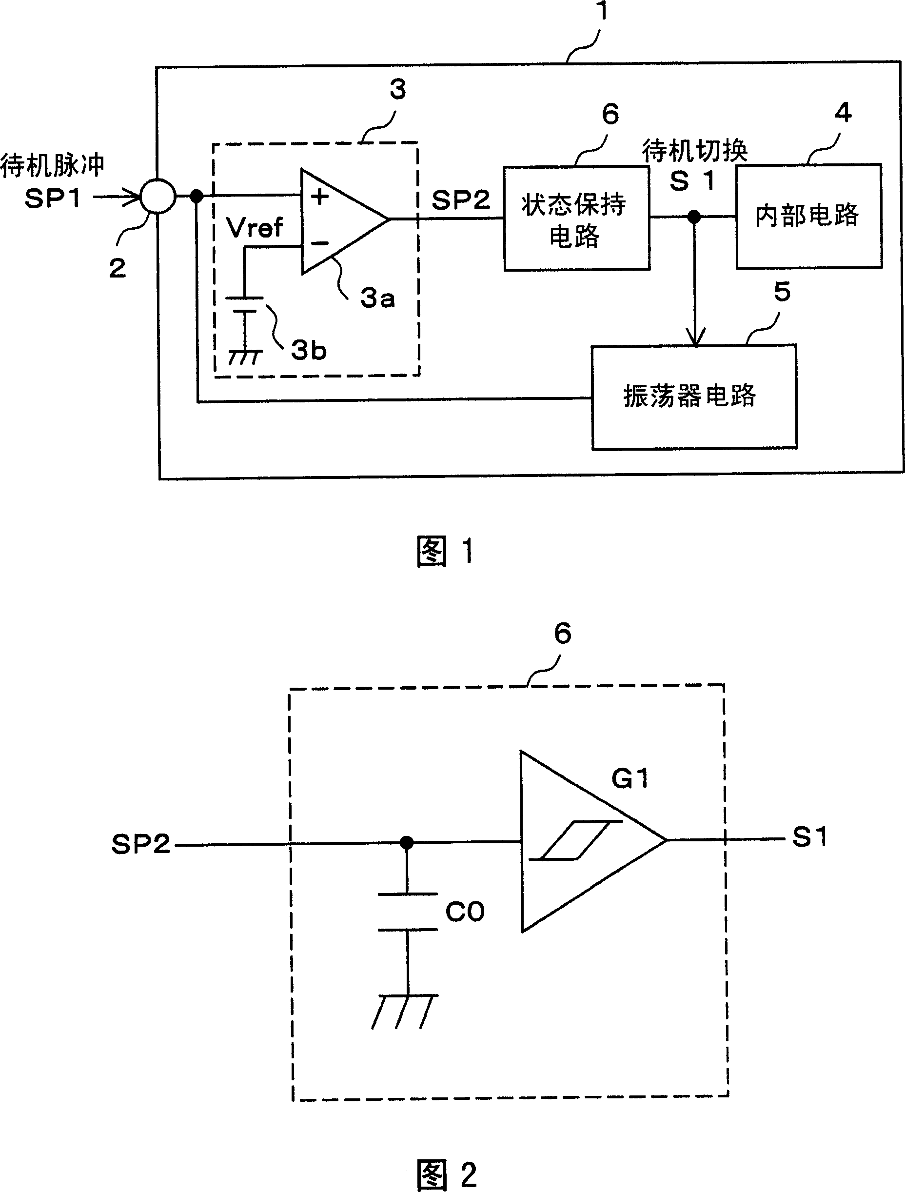
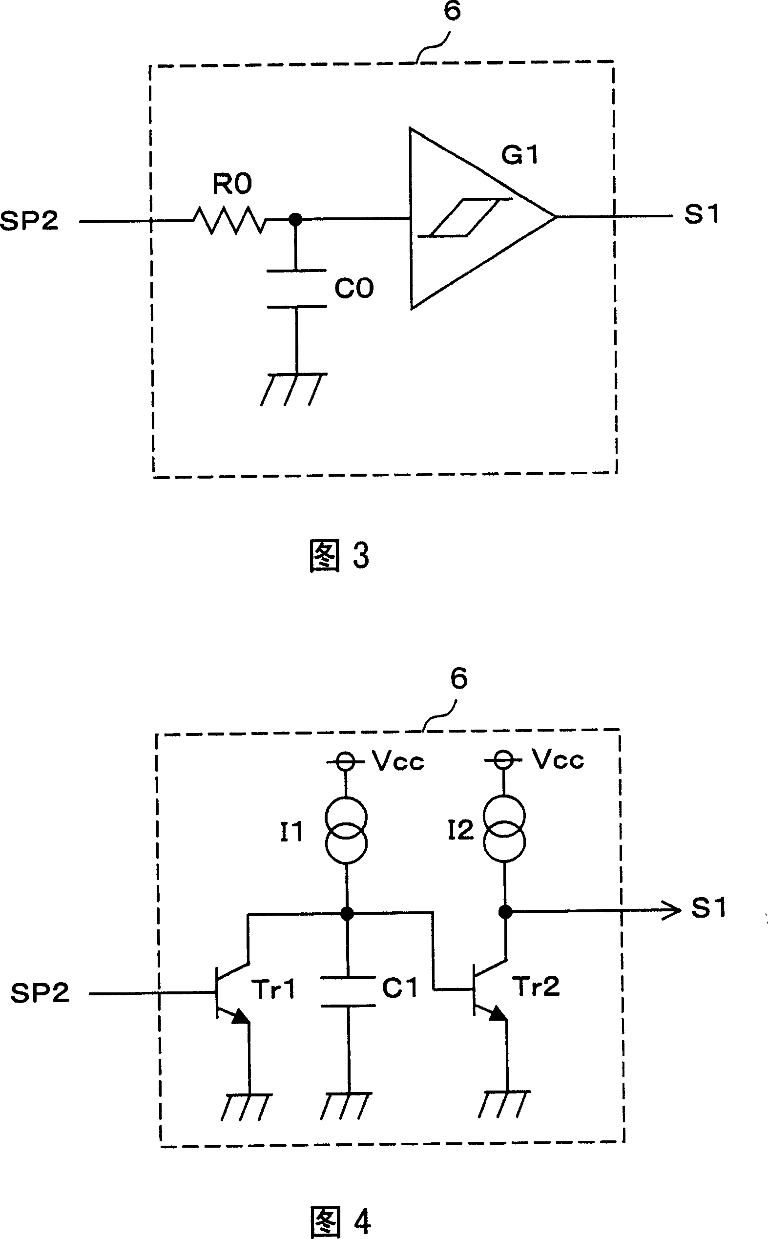
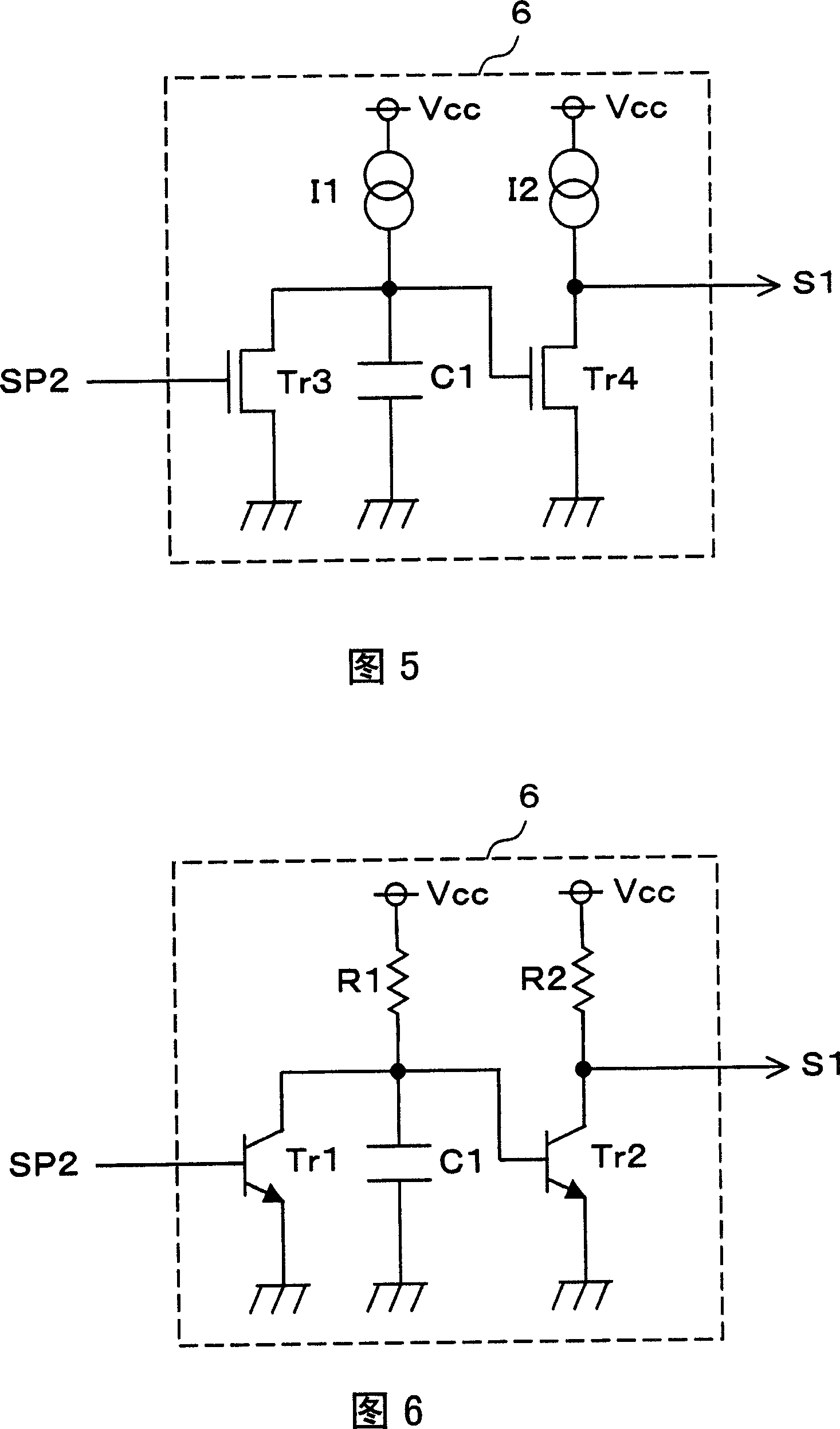
[0073] Hereinafter, embodiments of the present invention will be described with reference to the accompanying drawings. FIG. 1 is a block diagram schematically showing the configuration of an IC according to a first embodiment of the present invention. In FIG. 1, numeral 1 denotes an IC (semiconductor integrated circuit device) having a predetermined function. The IC 1 is configured with: a standby pulse input terminal 2 (signal input terminal), to which an external standby pulse signal SP1 is input; a comparator circuit 3, which compares the voltage of the standby pulse input terminal 2 with a reference voltage Vref; a state holding circuit 6. Based on the comparison result signal SP2, which is the output of the comparator circuit 3, a standby switching signal S1 is generated; the internal circuit 4, based on the standby switching signal S1, performs an on state in which a predetermined operation is performed and an off state in which the operation is stopped and the oscilla...


PUM


Abstract

An IC includes an internal circuit that switches between on-state and off-state in response to an external signal and also includes an oscillator circuit that is externally synchronized. The IC further includes a state holding circuit that, when pulses for synchronizing the oscillator circuit are inputted to a standby pulse input terminal, applies, to the internal and oscillator circuits, as an operation signal, a voltage obtained by rectifying pulses outputted from a comparator, and, when a constant voltage for non-operation is applied to the standby pulse input terminal for a given time period, applies, to the internal and oscillator circuits, as a non-operation signal, a constant voltage outputted from the comparator.

Description

technical field [0001] The present invention relates to a semiconductor integrated circuit device and a mobile device using the device. Specifically, the present invention relates to a semiconductor integrated circuit device equipped with a standby function, in order to reduce standby power, by an externally given standby signal, switching between an on state in which an operation is performed and an off state in which an operation is stopped, and The standby function also operates according to an externally supplied pulse signal. The present invention also relates to a mobile device using the semiconductor integrated circuit device. Background technique [0002] FIG. 11 is a block diagram schematically showing a conventional semiconductor integrated circuit device. In FIG. 11, numeral 50 denotes a semiconductor integrated circuit device (hereinafter referred to as IC (Integrated Circuit)) having a predetermined function. The IC50 is configured with: a standby input termi...

Claims


Application Information

Patent Timeline
IPC IPC(8): H03L3/00G06F1/04H02J1/00H03K17/00G06F1/12G06F1/32
CPCH02J9/005Y02B60/1225G06F1/12G06F1/3203G06F1/3275Y02B70/30Y04S20/20Y02D10/00
Inventor 冲宏一井手雄三
Owner ROHM CO LTD
Why Eureka
Try Eureka