Power-on solution to avoid crowbar current for multiple power supplies' inputs/outputs

Active Publication Date: 2006-10-05
SEMICON MFG INT (SHANGHAI) CORP
View PDF4 Cites 1 Cited by
  • Summary
  • Abstract
  • Description
  • Claims
  • Application Information

AI Technical Summary

Benefits of technology

[0006] According to the present invention, techniques directed to integrated circuits are provided. More particularly, the invention provides a method and device for avoiding crowbar current during power-on of integrated circuits. Merely by way of example, the invention has been applied to input/output (I/O) interfaces with multiple power supplies. But it would be recognized that the invention has a much broader range of applicability.
[0007] In a specific embodiment, the invention provides an integrated circuit. The integrated circuit includes a first node having a first supply voltage level. A first level shift circuit is connected between the first node and a first path. A second level shift circuit is connected between the first node and a second path. The first path includes an even number of inverter stages, while the second path includes an odd number of inverter stages. The first and second level shift circuits are configured to output a signal at the second supply voltage level. The integrated circuit also includes a PMOS transistor and an NMOS transistor connected in series between a second node having the second supply voltage level and a reference voltage. A gate of the PMOS transistor is connected to the first path, and a gate of the NMOS transistor is connected to the second path. An I/O pad connected between the PMOS and NMOS transistors has high impedance during a power-on period when the second node is powered up before the first node.
[0008] In another embodiment, an integrated circuit includes a first node having a first supply voltage level. A first level shift circuit is connected between the first node and a first path. A second level shift circuit is connected between the first node and a second path. The first path includes N, an even number, of inverter stages, while the second path includes N+1 inverter stages. The first and second level shift circuits are configured to output a signal at the second supply voltage level. The integrated circuit also includes a PMOS transistor and an NMOS transistor connected in series between a second node having the second supply voltage level and a reference voltage. A gate of the PMOS transistor is connected to the first path, and a gate of the NMOS transistor is connected to the second path. An I/O pad connected between the PMOS and NMOS transistors has high impedance during a power-on period when the second node is powered up before the first node.
[0009] In yet another embodiment, an integrate circuit includes a first node having a first supply voltage level. A first level shift circuit is connected between the first node and a first path. The first

Problems solved by technology

Increasing circuit density has improved performance and complexity of integrated circuits, but it has also introduced additional design constraints.
However, these smaller devices will sometimes interface or interoperate with larger devices of older technol

Method used


Image

  • Power-on solution to avoid crowbar current for multiple power supplies' inputs/outputs
  • Power-on solution to avoid crowbar current for multiple power supplies' inputs/outputs
  • Power-on solution to avoid crowbar current for multiple power supplies' inputs/outputs

Examples


Example

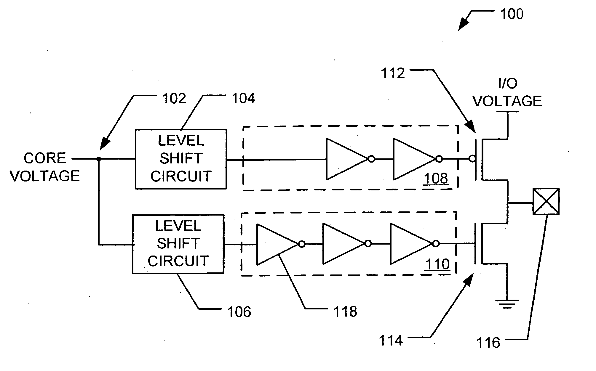
[0018] According to the present invention, techniques directed to integrated circuits are provided. More particularly, the invention provides a method and device for avoiding, or substantially reducing, crowbar current. Merely by way of example, the invention has been applied to I / O interfaces for integrated circuits with multiple power supplies. But it would be recognized that the invention has a much broader range of applicability.

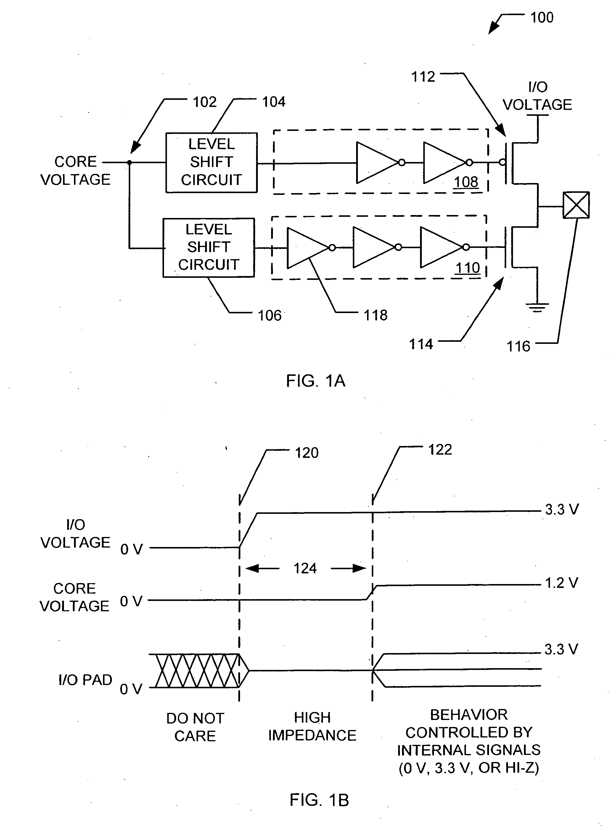
[0019]FIG. 1A is a simplified schematic of an integrated circuit 100 according to an embodiment of the present invention. This diagram is merely an example, which should not unduly limit the scope of the claims. One of ordinary skill in the art would recognize many variations, alternatives, and modifications. Integrated circuit 100 includes a node 102 at a core voltage, or a first supply voltage level. Upon power-on, core voltage increases over a short period of time from 0 volts to a predetermined voltage. In one embodiment, the predetermined voltage i...


PUM


Abstract

Techniques to avoid crowbar current are provided. An integrated circuit according to an embodiment of the present invention includes a first node having a first supply voltage level. A first level shift circuit is connected between the first node and a first path. A second level shift circuit is connected between the first node and a second path. The first path includes an even number of inverter stages, while the second path includes an odd number of inverter stages. The first and second level shift circuits are configured to output a signal at the second supply voltage level. The integrated circuit also includes a PMOS transistor and an NMOS transistor connected in series between a second node having the second supply voltage level and a reference voltage. A gate of the PMOS transistor is connected to the first path, and a gate of the NMOS transistor connected to the second path. An I/O pad connected between the PMOS and NMOS transistors has high impedance during a power-on period when the second node is powered up before the first node. In other specific embodiments, the inverter stages of the first path and the second path can be replaced with pull-up or pull-down circuits, respectively.

Description

BACKGROUND OF THE INVENTION [0001] The present invention is directed to integrated circuits and their processing for the manufacture of semiconductor devices. More particularly, the invention provides a method and device for avoiding crowbar current during power-on of integrated circuits. Merely by way of example, the invention has been applied to input / output (I / O) interfaces with multiple power supplies. But it would be recognized that the invention has a much broader range of applicability. [0002] Integrated circuits have evolved from a handful of interconnected devices fabricated on a single chip of silicon to millions of devices. Conventional integrated circuits provide performance and complexity far beyond what was originally imagined. In order to achieve improvements in complexity and circuit density (i.e., the number of devices capable of being packed onto a given chip area), the size of the smallest device feature, also known as the device “geometry”, has become smaller wit...

Claims


Application Information

Patent Timeline
IPC IPC(8): H03B1/00
CPCH03K19/0013
Inventor YU, TALEECHENG, HELLEN
Owner SEMICON MFG INT (SHANGHAI) CORP
Why Eureka
Try Eureka