
Optical device module, optical path fixing device, and method for manufacturing optical device module

a technology of optical components and optical components, applied in the field can solve the problems of interrupting the downsizing of optical device modules, low positioning accuracy of lenses and inconvenient assembly of optical components, so as to improve the positioning accuracy of optical components with respect to solid-state image sensors

Inactive Publication Date: 2006-10-05
SHARP KK
View PDF10 Cites 63 Cited by
  • Summary
  • Abstract
  • Description
  • Claims
  • Application Information

AI Technical Summary

Benefits of technology

[0014] The present invention has been devised in view of such circumferences and its object is to provide an optical device module configured in which a holding material for holding an optical component (a lens) of an optical path fixing device is fixed to a transparent cover adhered to the upper surface of a solid-state image sensor in a state of coming into contact with the same so that the positioning accuracy of the optical component with respect to the solid-state image sensor can be improved, and which the solid-state image sensor and the transparent cover are sealed in a synthetic resin thus to be protected from any external impact.
[0015] It is another object of the present invention to provide an optical device module configured for protection against external impacts, in which a wiring board and an signal processing device are sealed together with the solid-state image sensor and the transparent cover by a synthetic resin so that the signal processing device can be protected from any external impact.

Problems solved by technology

In a case where positioning accuracy of the lens with respect to the solid-state image sensor is low, problems occur such that the solid-state image sensor may be out of focus or a dim image of the object to be captured is generated.
However, as the adjusting mechanism which is used only in the assembling process is previously incorporated in the conventional optical device module, it will interrupt the downsizing of the optical device module.
Accordingly, any manufacturing error which is derived from the circuit board or the housing may interrupt the relative positional relationship of the lens to the solid-state image sensor.
When the package is deflected or distorted at its surface, which serves as a reference plane for adhering, by the effect of manufacturing error, it may interrupt the accuracy of positioning the lens relative to the image sensor.
In this prior art, however, since the signal processing device, the solid-state image sensor and the transparent cover are placed upon the substrate while the lens holding material is adhered to the transparent cover, the solid-state image sensor, the signal processing device and the like may be injured by any impact urged on the lens holding material.
It is however difficult to apply a uniform thickness of the adhesive at coating.
Since, at the time of adhering the lens holding material to the transparent cover, adhering portion is parallel to the upper surface of the transparent cover, that is, the radial direction of the lens, there is a fear that the optical path is intersected by overflowing excessive adhesive when adhesive is excessively coated.

Method used


Image

  • Optical device module, optical path fixing device, and method for manufacturing optical device module
  • Optical device module, optical path fixing device, and method for manufacturing optical device module
  • Optical device module, optical path fixing device, and method for manufacturing optical device module

Examples


Embodiment Construction

[0086] Preferred embodiments of the present invention will be described in more detail, referring to the relevant drawings.

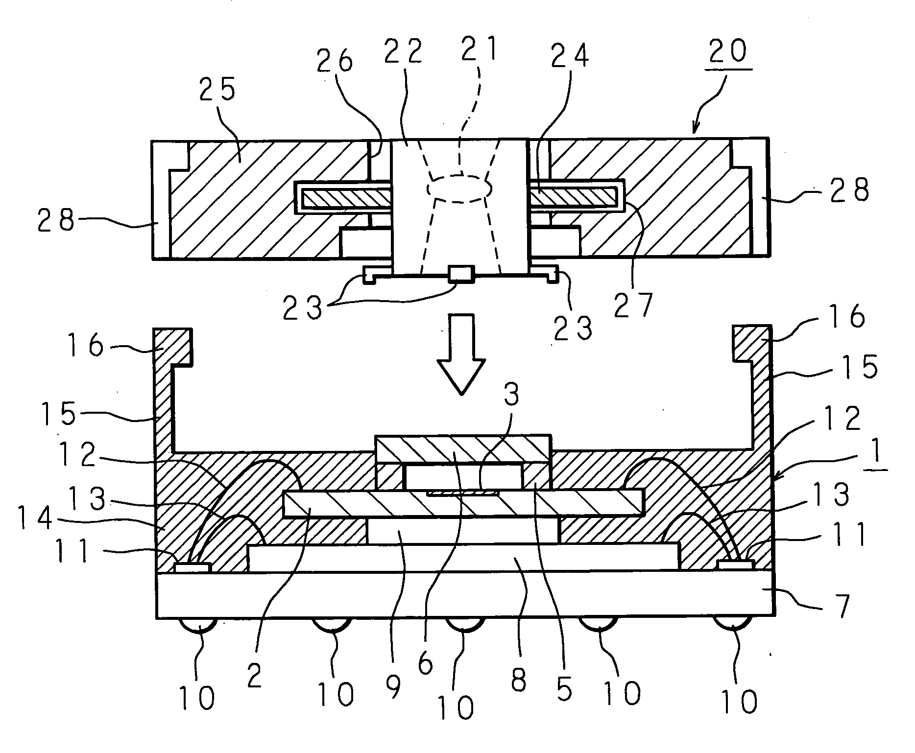
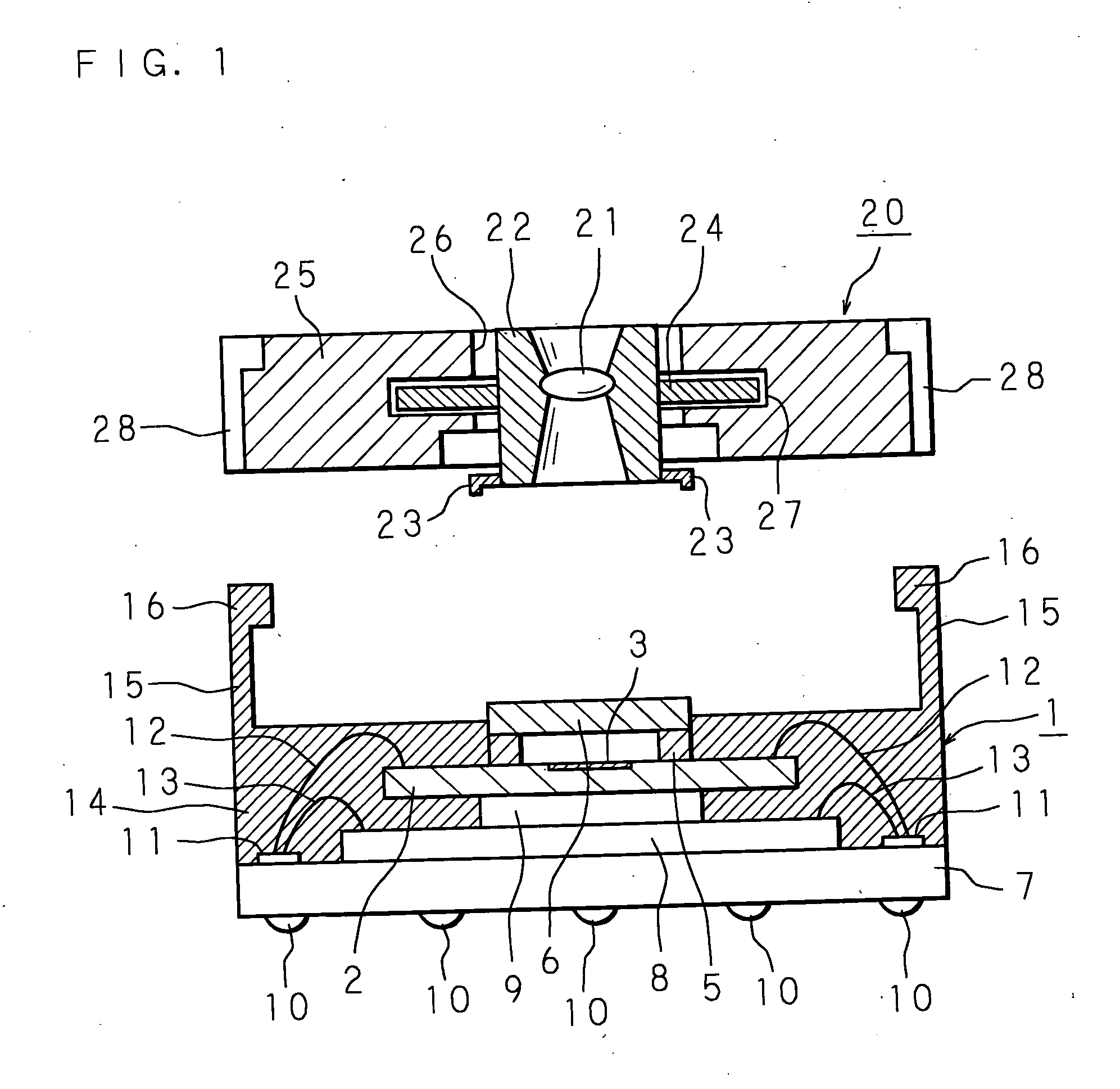
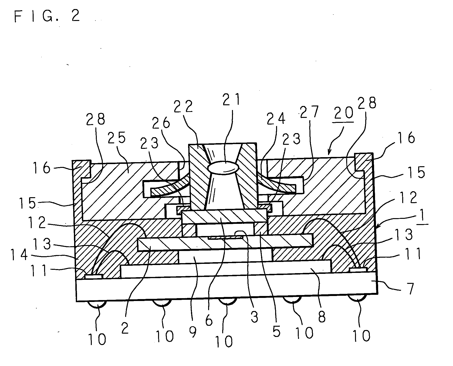
[0087]FIG. 1 and FIG. 2 are schematic cross sectional views of a configuration of an optical device module according to the present invention. More particularly, FIG. 1 illustrates a state where an optical path fixing device is not fixedly combined to an imaging unit of the optical device module, and FIG. 2 illustrates a state where the optical path fixing device is fixedly combined to the same.

[0088]FIG. 3 is a schematic plan view of a solid-state image sensor of the optical device module of the present invention. FIG. 4 is a schematic perspective view showing an external appearance of the optical device module of the present invention. FIG. 5 is a schematic plan view showing an external appearance of the optical device module of the present invention. FIG. 6 is a schematic perspective view showing a holding material of the optical path fixing device of the o...


PUM


Abstract

A solid-state image sensor, a transparent cover, a DSP, a wiring board and the like are sealed in a sealing portion by molding of a synthetic resin, and fixed to an imaging unit. At this time, a portion of the transparent cover is exposed from the sealing portion. The optical path fixing device and the imaging unit sealed by the sealing portion are fixedly combined by engagement of hook engaging portions and hook portions, in a state where the lower end surface of a lens barrel comes into contact with the exposed portion. As the result, positioning accuracy of a lens with respect to a pixel area of the solid-state image sensor dose not deteriorate even if a substrate on which the solid-state image sensor is arranged is deflected or distorted.

Description

CROSS-REFERENCE TO RELATED APPLICATIONS [0001] This non-provisional application claims priority under 35 U.S.C. §119(a) on Patent Application No. 2005-95573 filed in Japan on Mar. 29, 2005, the entire contents of which are hereby incorporated by reference. BACKGROUND OF THE INVENTION [0002] 1. Field of the Invention [0003] The present invention relates to an optical device module which is provided with a solid-state image sensor for photographing an object and is built in a digital camera, mobile phone with camera, digital video camera or the like, and relates to an optical path fixing device built in such an optical device module for fixing an optical path to the solid-state image sensor, further more, relates to a method for manufacturing such optical device module as described above. [0004] 2. Description of Related Art [0005] A solid-state image sensor for use in a digital camera or a mobile phone with camera is used for capturing image of an object to be photographed and provid...

Claims


Application Information

Patent Timeline
IPC IPC(8): H04N5/225G02B7/02G03B17/02H01L27/14H04N5/335
CPCH01L27/14618H01L27/14625H01L31/0203H01L2224/48227H01L2924/15311H01L2924/1815H01L2924/3025H01L2224/48091H01L2924/00014H01L2924/00H04N23/57H01L27/14H04N25/00
Inventor TSUKAMOTO, HIROAKIHIROSUMI, NOBUHITOYASUDOME, TAKASHIKINOSHITA, KAZUO
Owner SHARP KK
Learn More