Packaging substrate having adhesive-overflowing prevention structure

Inactive Publication Date: 2006-10-05
LINGSEN PRECISION INDS
3 Cites 17 Cited by

AI-Extracted Technical Summary

Problems solved by technology

During installation of the passive component, the bonding adhesive may be forced to overflow on the surface o...

Method used

[0016] By means of the arrangement of the aforesaid first and second embodiments of the present invention, the bonding adhesive will be guided into the overflow-preventive grooves...

Benefits of technology

[0007] The present invention has been accomplished under the circumstances in view. It is one object of the present invention to provide a packaging substra...

Abstract

A packaging substrate includes an array of packaging units. Each packaging unit has a chip pad carrying a chip, a plurality of pins arranged around the chip pad and spaced from one another and the chip pad by an open space, an insulative member filling up the open space, passive components each connected between two pins, a bonding adhesive applied to the pins to which the passive components is connected to affix the connection between the passive components and the respective pins, and a plurality of overflow-preventive grooves respectively provided around the bonding adhesive at each of the pins to which the passive components are connected to prevent overflow of the bonding adhesive.

Application Domain

Printed circuit assemblingFinal product manufacture +9

Technology Topic

AdhesiveElectrical and Electronics engineering

Image

  • Packaging substrate having adhesive-overflowing prevention structure
  • Packaging substrate having adhesive-overflowing prevention structure
  • Packaging substrate having adhesive-overflowing prevention structure

Examples

  • Experimental program(1)

Example

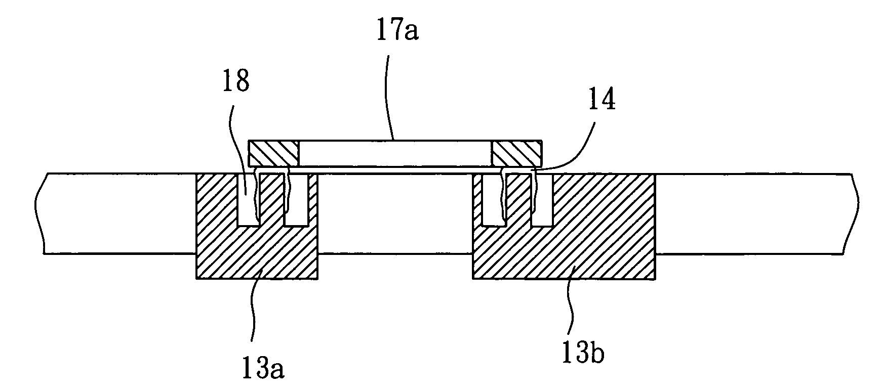
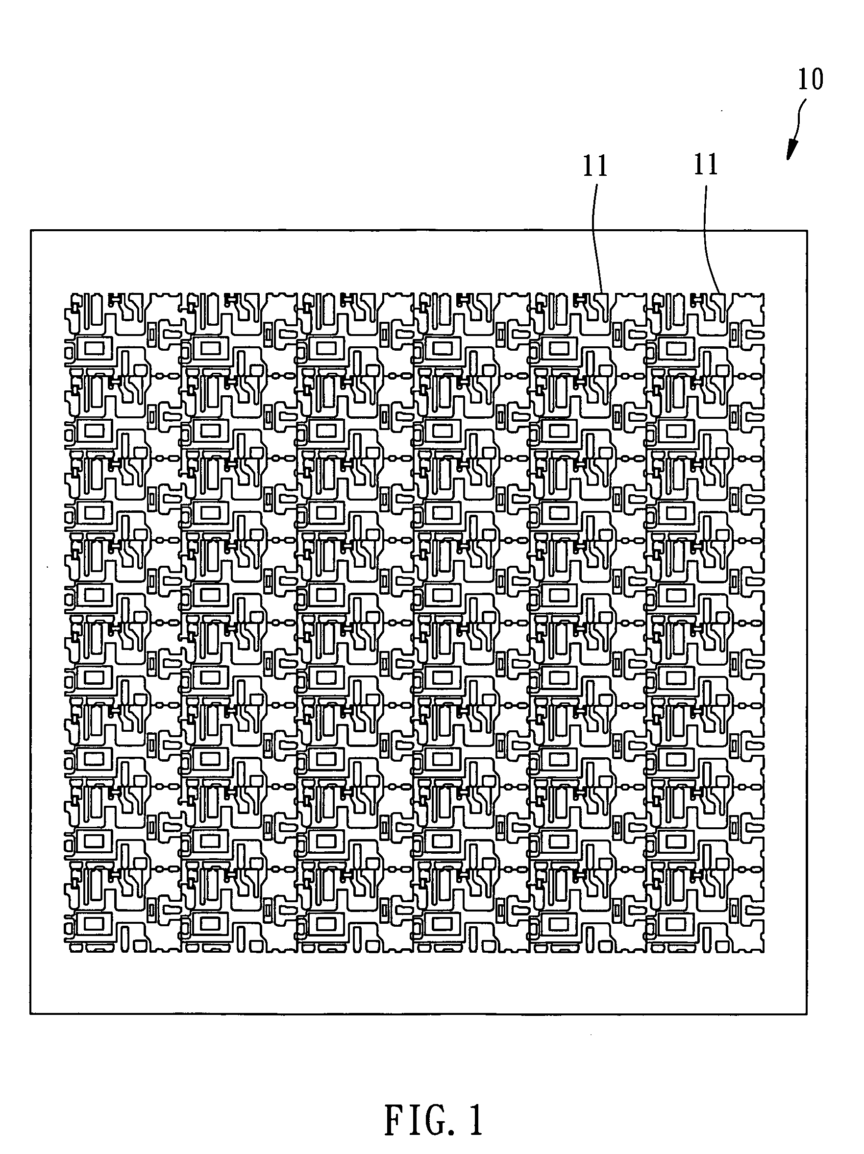
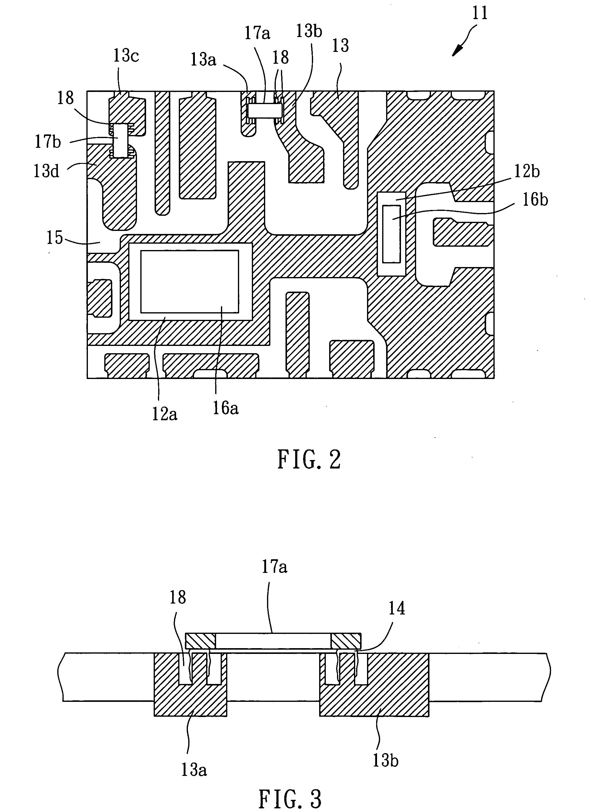
[0013] Referring to FIGS. 1-3, a packaging substrate in accordance with the first preferred embodiment of the present invention is shown comprising a plurality of packaging units 11 arranged in an array. The packaging units 11 have a flat, rectangular shape, each comprised of two chip pads 12a and 12b, a plurality of pins 13, an insulative member 15, two passive components 17a and 17b, and a plurality of overflow-preventive grooves 18.
[0014] The chip pads 12a and 12b each carry a chip 16a or 16b. The pins 13 are arranged along the border of the respective packaging unit 11 around the chip pads 12a. and 12b. The pins 13 are respectively spaced from the chip pad 12a and spaced from one another by openings. The insulative member 14 fills up the openings between the pins 13 and the chip pads 12a and 12b between each two adjacent pins 13, thereby forming with the pins 13 and the chip pads 12a and 12b a unitary platform. Further, a bonding adhesive 14 (for example, tin paste) is applied to four pins 13a, 13b, 13c, and 13d that are arranged in two pairs (only one pair of pins 13a and 13b is shown in FIG. 3). The two passive components 17a and 17b, which can be resistors, capacitors, or inductors, are respectively connected between the respective pair of pins 13a and 13b, or 13c and 13d and bonded to the bonding adhesive 14 at the respective pins. The overflow-preventive grooves 18 are straight grooves arranged in pairs respectively disposed at two sides of the bonding adhesive 14 at each of the pins 13a, 13b, 13c, and 13d.
[0015]FIG. 4 shows a packaging substrate according to the second preferred embodiment of the present invention. This embodiment is substantially similar to the aforesaid first embodiment with the exception that the overflow-preventive grooves 18 are annular grooves respectively surrounding the bonding adhesive 14 at each of the pins 13a, 13b, 13c, and 13d.
[0016] By means of the arrangement of the aforesaid first and second embodiments of the present invention, the bonding adhesive will be guided into the overflow-preventive grooves when pressed by the passive components during the installation of the passive components, thereby preventing an overflow of the bonding adhesive on the surface of the substrate.
[0017] Although particular embodiments of the invention have been described in detail for purposes of illustration, various modifications and enhancements may be made without departing from the spirit and scope of the invention. Accordingly, the invention is not to be limited except as by the appended claims

PUM

no PUM

Description & Claims & Application Information

We can also present the details of the Description, Claims and Application information to help users get a comprehensive understanding of the technical details of the patent, such as background art, summary of invention, brief description of drawings, description of embodiments, and other original content. On the other hand, users can also determine the specific scope of protection of the technology through the list of claims; as well as understand the changes in the life cycle of the technology with the presentation of the patent timeline. Login to view more.

Similar technology patents

Semiconductor device having a filling pattern around a storage structure and method of forming the same

InactiveUS20090134525A1prevent short-circuitingincrease alignment margin
Owner:SAMSUNG ELECTRONICS CO LTD

Photoelectric conversion module and method of manufacturing the same

InactiveUS20120012158A1prevent short-circuiting
Owner:SAMSUNG SDI CO LTD

Printed circuit boards having improved solder pads

InactiveUS20050282415A1improve solder pad layoutprevent short-circuiting
Owner:HON HAI PRECISION IND CO LTD

Non-aqueous electrolyte battery

InactiveUS7510799B2improve sealing characteristicprevent short-circuiting
Owner:MURATA MFG CO LTD

Plasma display panel

InactiveUS20090134795A1prevent short-circuitingprevent problem
Owner:SAMSUNG SDI CO LTD

Classification and recommendation of technical efficacy words

  • prevent short-circuiting

Connector, jack socket component, electronic equipment and plug component

InactiveUS20090061694A1prevent short-circuiting
Owner:LENOVO INNOVATIONS LTD HONG KONG

Multilayer Printed Wiring Board And Manufacturing Method For Same

InactiveUS20080121416A1prevent short-circuitingmanufacture very thin
Owner:PANASONIC CORP

Semiconductor device comprising electromigration prevention film and manufacturing method thereof

ActiveUS20080191357A1prevent short-circuiting
Owner:AOI ELECTRONICS CO LTD

Electric connector having power cable retaining structure

InactiveUS7338306B1prevent short-circuiting
Owner:CHEN JUI LUNG

Non-aqueous electrolyte battery

InactiveUS7510799B2improve sealing characteristicprevent short-circuiting
Owner:MURATA MFG CO LTD
Why Eureka
Try Eureka