Solid-state imaging device

Inactive Publication Date: 2006-10-12
PANASONIC CORP
View PDF39 Cites 33 Cited by
  • Summary
  • Abstract
  • Description
  • Claims
  • Application Information

AI Technical Summary

Benefits of technology

[0027] Due to the above, in the solid-state imaging device according to the present invention, the surface side interface of the p-well is located in an area deeper than in the conventional device. Thus, the solid-state imaging device according to the present invention suppresses the emission of electrons stored in the photodiode to the back surface of the semiconductor substrate and emits electrons generated in the area deeper than the p-well to the back surface

Problems solved by technology

Therefore, in the CCD imaging device, electrons generated by the photoelectric conversion may leak, causing a problem of deteriorating image quality.
More specifically, the CCD imaging device has a problem of easily developing phenomena such as smear, blooming and color mixture.
However, the MOS imaging device cannot suppress blooming and color mixture completely.
Therefore, there is a problem that the MOS imaging device shown in FIG

Method used


Image

  • Solid-state imaging device
  • Solid-state imaging device
  • Solid-state imaging device

Examples


embodiment 1

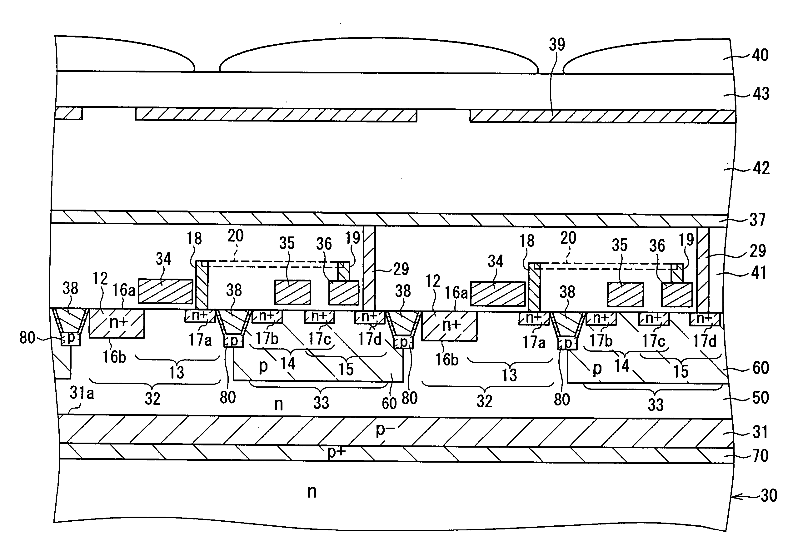
[0049] The following is a description of a solid-state imaging device according to Embodiment 1 of the present invention, with reference to FIGS. 1 to 3. The solid-state imaging device according to Embodiment 1 is a MOS imaging device and has a circuit configuration similar to the conventional MOS imaging device shown in FIG. 12 except for its cross-sectional structure. This will be described in the following.

[0050] The cross-sectional structure of the solid-state imaging device according to Embodiment 1 will be described referring to FIG. 1. FIG. 1 is a sectional view showing the structure of the solid-state imaging device according to Embodiment 1 of the present invention. As shown in FIG. 1, a p-well 31 is formed in a semiconductor substrate 30 so as to overlap photoelectric conversion portions 32 and signal detection portions 33 when viewed in a thickness direction of the semiconductor substrate 30. In other words, the p-well 31 is formed so that its formation region overlaps a...

embodiment 2

[0073] Now, a solid-state imaging device according to Embodiment 2 of the present invention will be described, with reference to FIGS. 4 and 5. The solid-state imaging device according to Embodiment 2 also is a MOS imaging device and has a circuit configuration similar to the conventional MOS imaging device shown in FIG. 12.

[0074] First, the cross-sectional structure of the solid-state imaging device according to Embodiment 2 will be described referring to FIG. 4. FIG. 4 is a sectional view showing the structure of the solid-state imaging device according to Embodiment 2 of the present invention. In FIG. 4, portions assigned the reference numerals indicated in FIG. 1 are similar to the portions shown in FIG. 1.

[0075] As shown in FIG. 4, in Embodiment 2, second p-wells 60 whose surface side interface coincides with the substrate surface are formed above the p-well 31 in the semiconductor substrate 30. The second p-wells 60 overlap only the signal detection portions 33 when viewed i...

embodiment 3

[0088] Now, a solid-state imaging device according to Embodiment 3 of the present invention will be described, with reference to FIG. 6. The solid-state imaging device according to Embodiment 3 also is a MOS imaging device and has a circuit configuration similar to the conventional MOS imaging device shown in FIG. 12. FIG. 6 is a sectional view showing the structure of the solid-state imaging device according to Embodiment 3 of the present invention. In FIG. 6, portions assigned the reference numerals indicated in FIGS. 1 and 4 are similar to the portions shown in FIGS. 1 and 4.

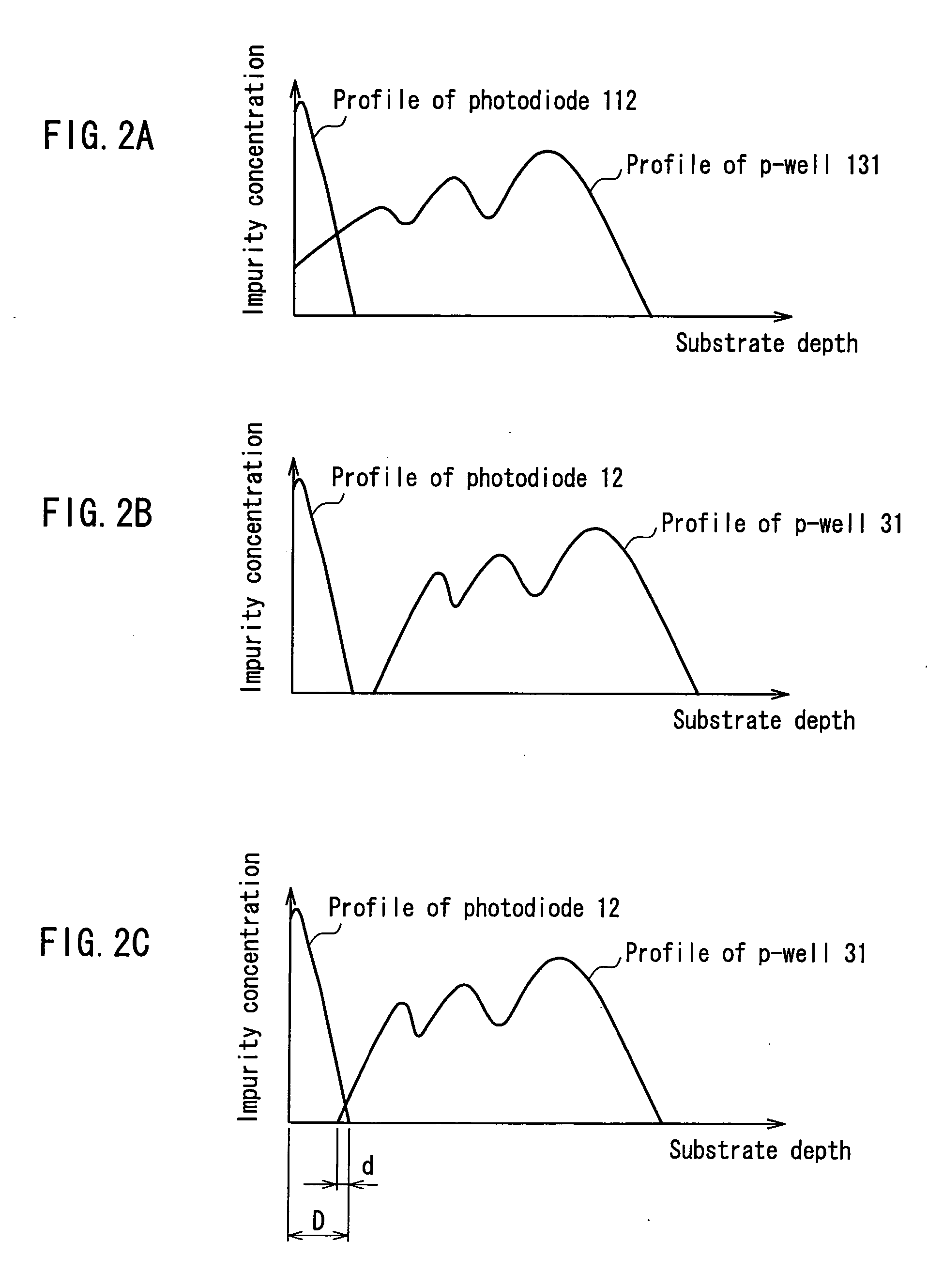
[0089] As shown in FIG. 6, in Embodiment 3, a p-type buried region 70 having a higher impurity concentration than the p-well 31 is formed below the p-well 31 in the semiconductor substrate 30. The surface side interface of the buried region 70 coincides with the lower side interface of the p-well 31. Further, it is preferable that the impurity concentration of the buried region 70 is set to, for example, 1×1...


PUM


Abstract

A solid-state imaging device including an n-type semiconductor substrate including a photoelectric conversion portion, and a signal detection portion for detecting a signal charge is used. The photoelectric conversion portion is provided with a photodiode, and a p-well that overlaps the photoelectric conversion portion and the signal detection portion when viewed in a thickness direction of the semiconductor substrate is formed in the semiconductor substrate. The p-well is formed so that a surface side interface is located below a surface side interface of the photodiode. Preferably, the surface side interface of the p-well is located below a lower side interface of the photodiode and an impurity profile of the p-well does not overlap that of the photodiode. At this time, a non-dope region is present between the photodiode and the p-well.

Description

BACKGROUND OF THE INVENTION [0001] 1. Field of the Invention [0002] The present invention relates to a solid-state imaging device. [0003] 2. Description of Related Art [0004] Conventionally, MOS imaging devices and CCD (charge coupled device) imaging devices are known as prominent solid-state imaging devices. Among them, in a MOS imaging device, incident light is converted into a signal charge by a photoelectric conversion region (a photodiode), and the signal charge is amplified by a transistor. More specifically, the potential of the photoelectric conversion region is modulated by the signal charge generated from the photoelectric conversion. Then, the amplification coefficient of the amplifying transistor varies according to that potential. [0005] Also, in the case of the MOS imaging device, the transistor for amplifying the signal charge is included in a pixel portion. Accordingly, the MOS imaging device easily can be adapted to a decrease in pixel size and an increase in the nu...

Claims


Application Information

Patent Timeline
IPC IPC(8): H01L31/111H01L31/06H01L27/146H01L31/10H04N5/335H04N5/359H04N5/369H04N5/374
CPCH01L27/14609H01L27/14627H01L27/14689H01L27/14643H01L27/14654H01L27/1463
Inventor KATSUNO, MOTONARIMATSUNAGA, YOSHIYUKI
Owner PANASONIC CORP
Why Eureka
Try Eureka