Optical modulator with coupled coplanar strip electrode and domain inversion

an optical modulator and coplanar strip technology, applied in the field of optical modulators with coupled coplana, can solve the problems of uneven overlap efficiency between the two mzi waveguide arms, electrical confinement, etc., and achieve the effects of reducing voltage-length products, modest line impedance reduction, and improving performan

Inactive Publication Date: 2006-10-12
PHOTONICSYST
View PDF5 Cites 22 Cited by
  • Summary
  • Abstract
  • Description
  • Claims
  • Application Information

AI Technical Summary

Benefits of technology

[0017] The optical modulator of the invention is characterized by reduced voltage-length products at the cost of modest reduction in line impedance and can be used to design lower voltage analog devices, which, in turn, make practical the introduction of new analog links. In digital applications, the optical modulator of the invention can be incorporated in shorter devices and smaller platforms. With respect to uncoupled, do

Problems solved by technology

In the “push-pull” configuration associated with the CPW arrangement disclosed in U.S. Pat. No. 6,304,685 B1 and U.S. Pat. No. 6,356,

Method used


Image

  • Optical modulator with coupled coplanar strip electrode and domain inversion
  • Optical modulator with coupled coplanar strip electrode and domain inversion
  • Optical modulator with coupled coplanar strip electrode and domain inversion

Examples


Embodiment Construction

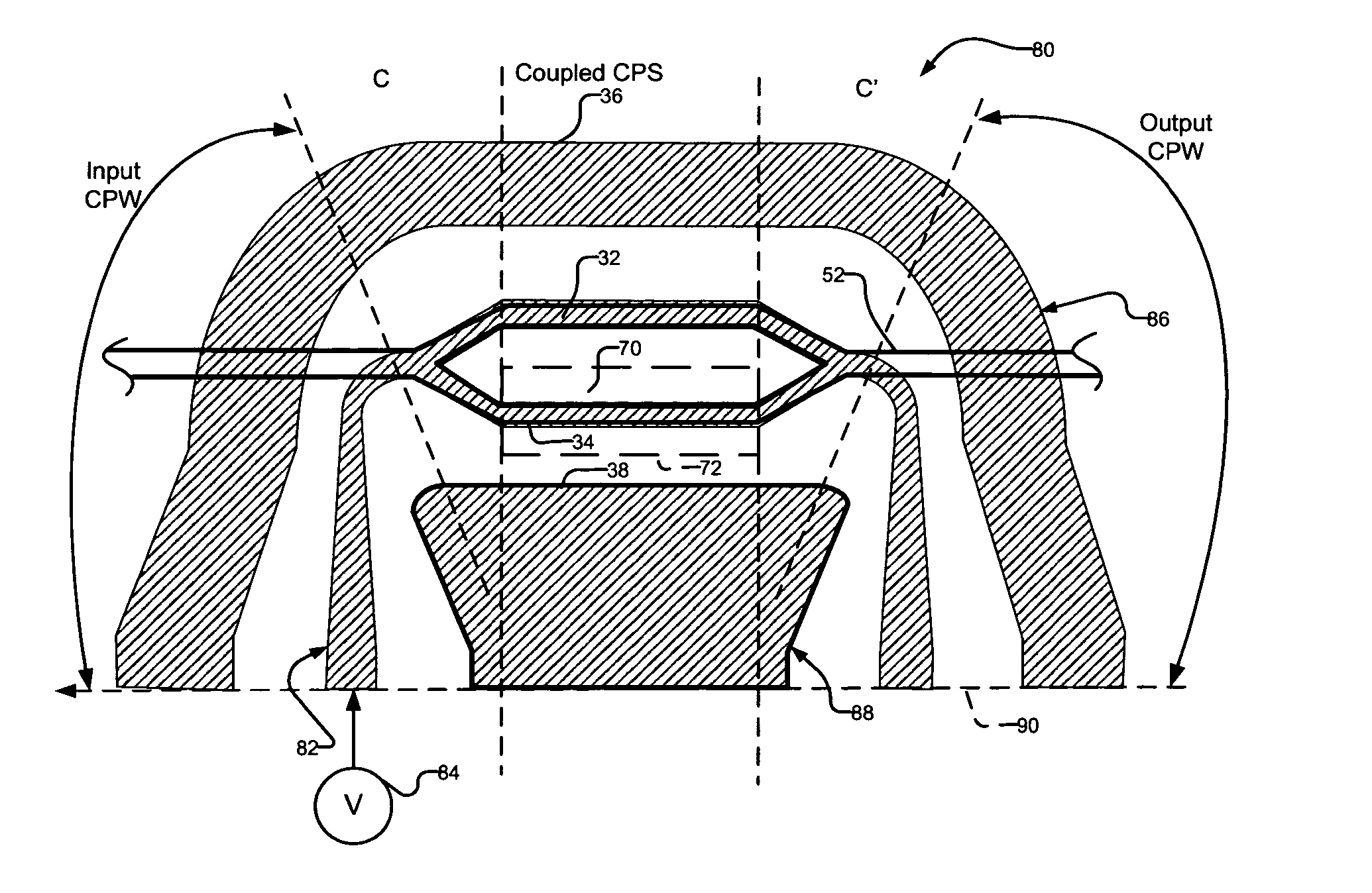
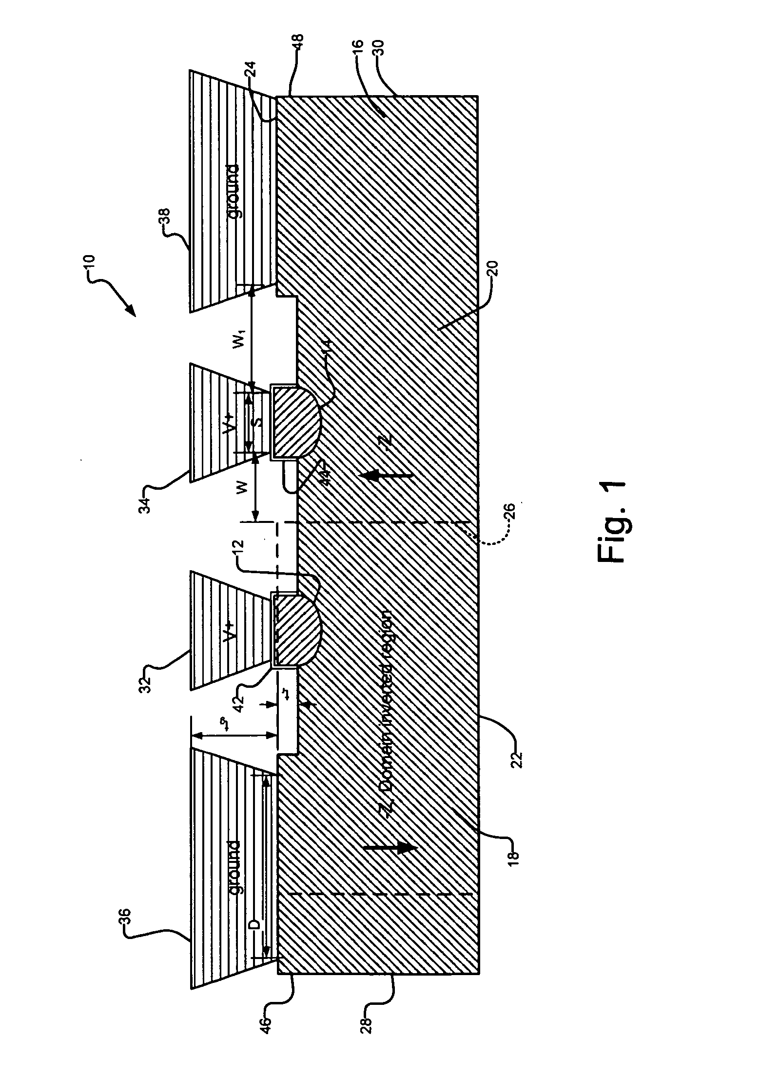
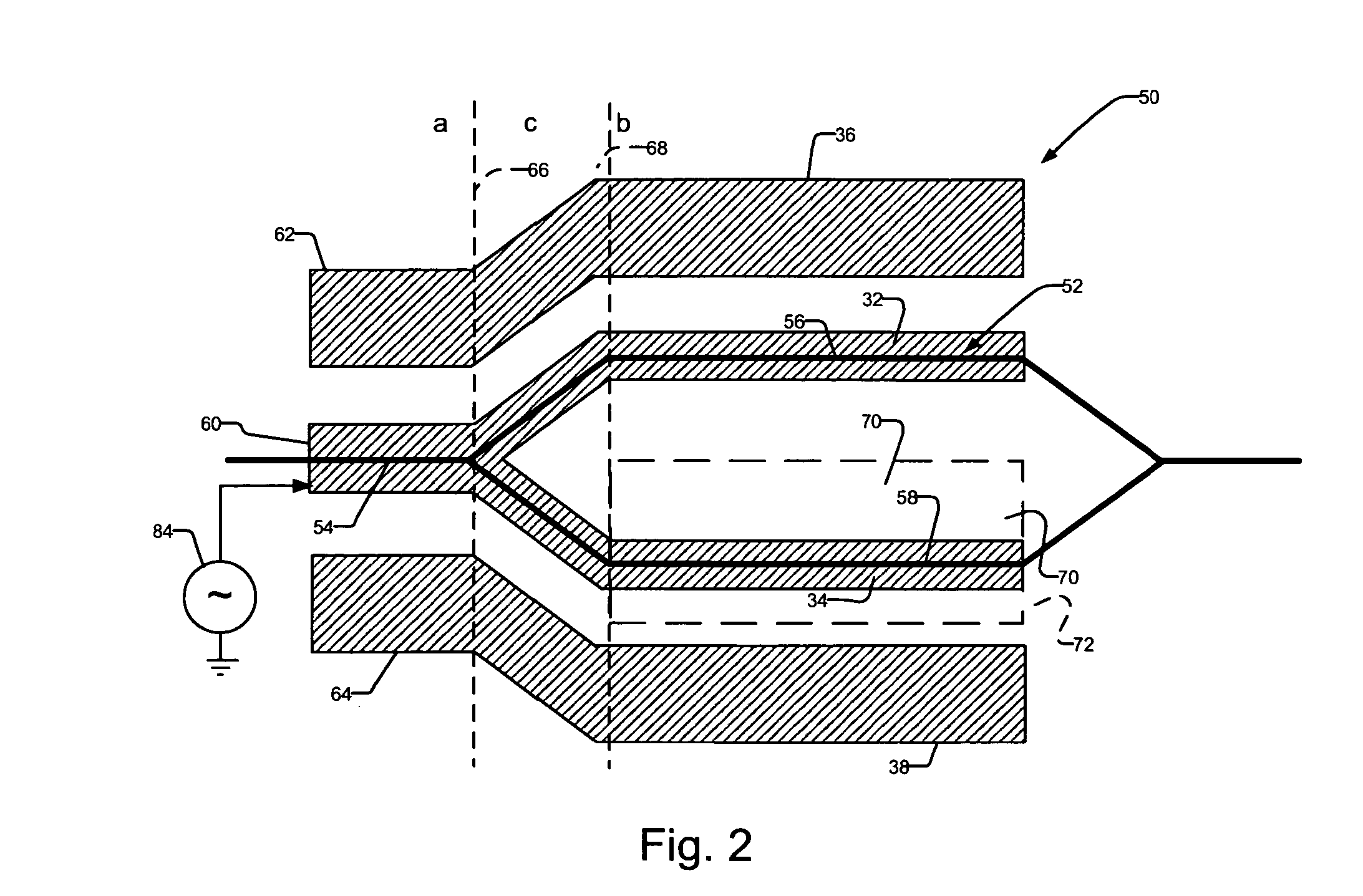
[0026] The invention is related to a modulator that includes an interferometer waveguide structure formed on an electro-optical substrate that has at least one domain inversion. Coupled electrodes extend, respectively, near a first and second arm of the interferometer waveguide structure.

[0027] Shown in FIG. 1 is a cross sectional view of modulator 10, which includes arms 12 and 14 of an interferometer waveguide structure, formed on substrate 16. The interferometer waveguide structure, for example a MZI, can be formed by techniques known in the art. For instance, a strip of titanium (Ti) metal can be deposited on an electro-optical blank. At high temperatures, Ti diffuses into the blank, forming the waveguide structure.

[0028] Generally, substrate 16 has a thickness in the range of from about 0.1 mm and about 1 mm. Preferably, it is formed of Z-cut LiNbO3. In a Z-cut substrate, the z (also called the c) crystal axis is normal to the substrate surfaces having the largest area. In ot...


PUM


Abstract

A modulator includes an interferometer waveguide structure formed on an electro-optical substrate, preferably a Z-cut lithium niobate or a Z-cut lithium tantalate. The substrate includes a domain inversion between a region near the first arm and a region near the second arm of the interferometer waveguide structure. In one example, two coplanar strip electrode structures, each extending near at least a portion of the first arm and the second arm, respectively, are electrically coupled to each other.

Description

BACKGROUND OF THE INVENTION [0001] Mach Zehnder interferometers (MZIs) are used to modulate the amplitude or intensity of an optical signal, for instance in digital and analog communications and electric field sensors. Often, they are fabricated as monolithic devices on either Z-cut or X-cut lithium niobate or lithium tantalate. [0002] A typical MZI includes two arms for dividing an optical input signal into two beams, which are then recombined. In one design, the arms have equal length. During operation, the relative phase of the two beams is controlled by some type of optical phase modulation in one or both arms in order to modulate the intensity of the output signal, which depends on the relative phase of the two beams. [0003] In many applications, the drive voltage of the modulator is of particular interest as it affects link gain, sensor sensitivity, and drive power requirements for high speed, such as ˜40 Gigahertz (GHz) or faster, analog or digital links. Drive voltage sensit...

Claims


Application Information

Patent Timeline
IPC IPC(8): G02F1/035
CPCG02F1/0356G02F2001/212G02F1/2255G02F1/212
Inventor BURNS, WILLIAM K.
Owner PHOTONICSYST
Why Eureka
Try Eureka