Apparatus and method for cleaning a semiconductor wafer

a technology of apparatus and semiconductor wafer, which is applied in the direction of chemistry apparatus and processes, cleaning using liquids, toys, etc., can solve the problems of contaminants contaminating, spin dryer, and contaminants remaining in the chamber, and achieve the effect of enhancing drying efficiency, reducing surface tension of deionized water on the wafer, and easily removing deionized water from the wafer

Inactive Publication Date: 2006-10-19
SAMSUNG ELECTRONICS CO LTD
View PDF8 Cites 41 Cited by
  • Summary
  • Abstract
  • Description
  • Claims
  • Application Information

AI Technical Summary

Benefits of technology

[0019] According to the above, the drying process is carried out while the processing chamber is in the organic solvent atmosphere, and thus the surface tension of the deionized water on the wafer may be greatly reduced, thereby easily removing the deionized water from the wafer.
[0020] Further, the organic solvent atmosphere in the container, the concentration of the organic solvent on the entire surface of the wafer and the temperature of the wafer may be controlled using the controller, thereby enhancing the drying efficiency and reducing the process time required to dry the wafer.

Problems solved by technology

However, as structures of the semiconductor chips increase the complexity thereof, the spin dryer showed limitations in that tiny water droplets on the wafer surface were not completely removed by the spin dryer, but the contaminants aggregated in the tiny water droplets are remained on the wafer surface.
However, since a group of wafers is substantially simultaneously dried in the multi-wafer dryer, contaminants remain in the chamber after the drying process is finished.
These contaminants contaminate a next group of wafers transferred into the chamber for the drying process.
This problem is especially serious with the multi-wafer dryer that uses a single chamber for the chemical treatment process, the rinsing process, and the drying process.
Therefore, the meniscus layer tends to be unstable, resulting poor drying, and the deionized water within a fine structure such as a contact hole is not easily removed with the single-wafer dryer.
Another problem with the single-wafer dryer is that local dry spots are formed easily on the wafer surface.

Method used


Image

  • Apparatus and method for cleaning a semiconductor wafer
  • Apparatus and method for cleaning a semiconductor wafer
  • Apparatus and method for cleaning a semiconductor wafer

Examples


Embodiment Construction

[0031] Hereinafter, the embodiments of the present invention will be described below in more detail with reference to the accompanying drawings, FIGS. 1 to 13. The present invention may, however, be embodied in different forms and should not be constructed as limited to the embodiments set forth herein. Rather, these embodiments are provided so that this disclosure will be thorough and complete, and will fully convey the scope of the invention to those skilled in the art.

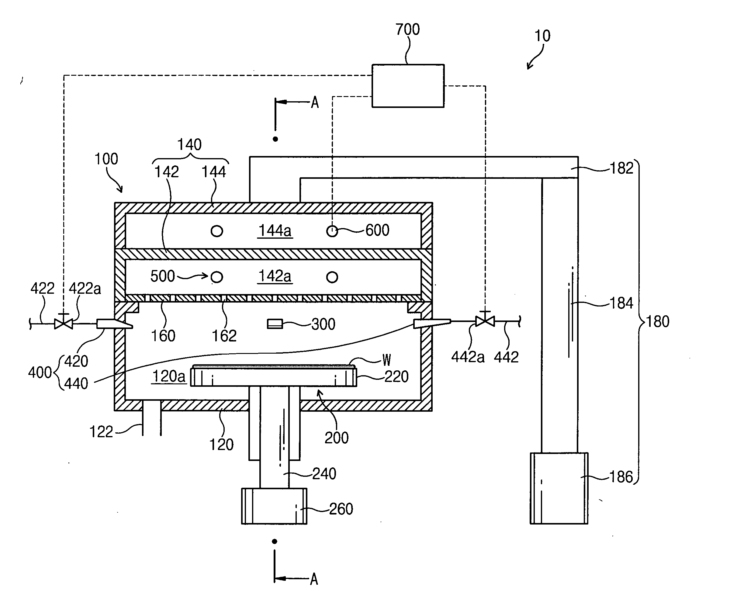
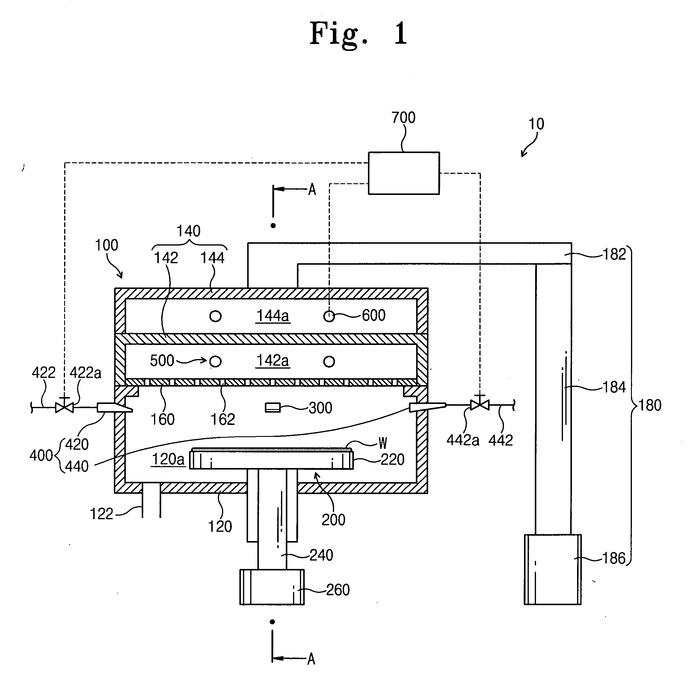
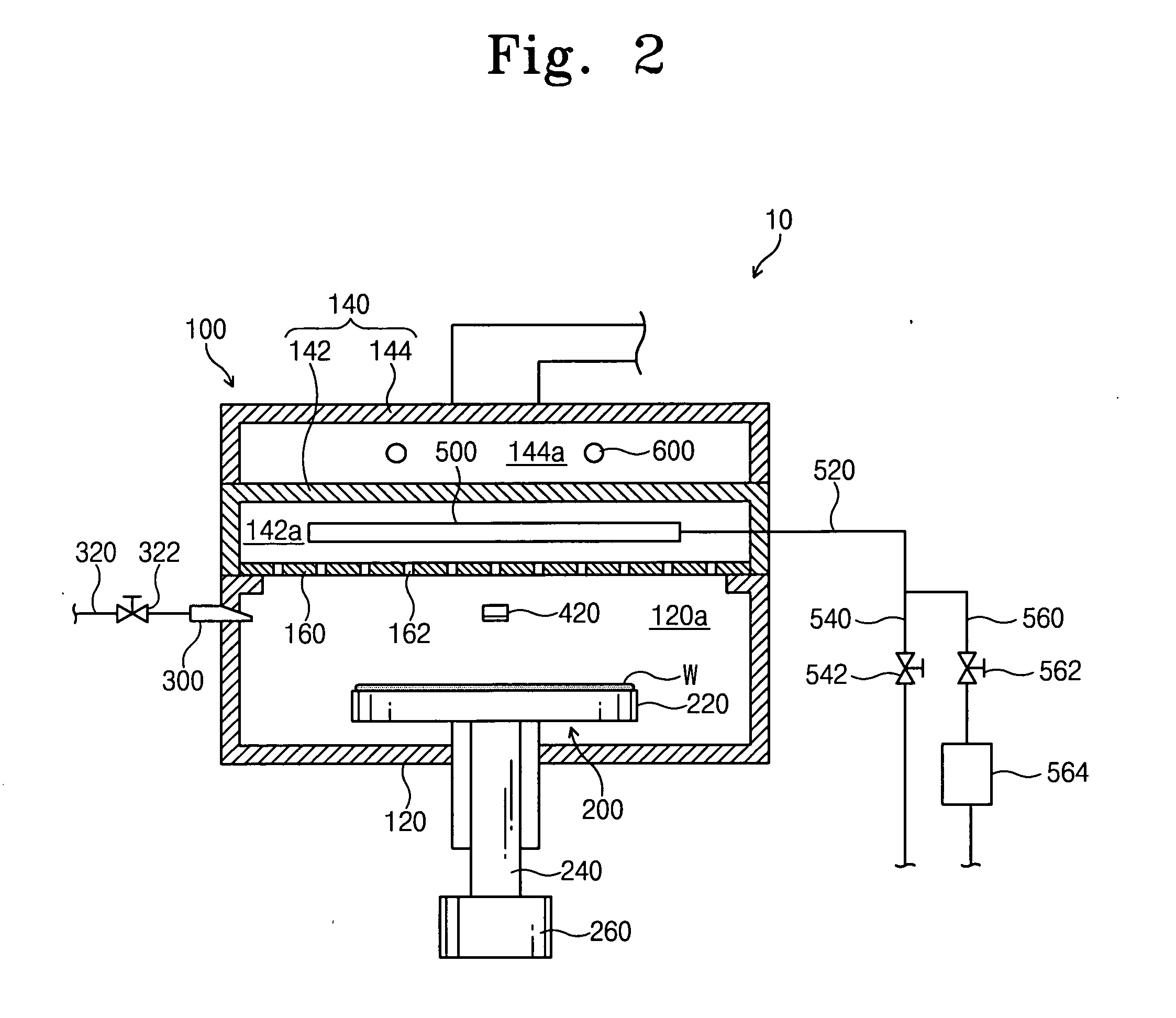
[0032] Referring to FIGS. 1 and 2, the cleaning apparatus 10 includes a process chamber 100, a supporter apparatus 200, a rinsing nozzle 300, an organic solvent supplying nozzle 400, a dry gas supplying nozzle 500 and a heater 600.

[0033] The process chamber 100 defines a work space for a cleaning process. The process chamber 100 includes a container 120 and a lid 140. The container 120 has an inner space 120a therein with an opening at its top. An exhaust line 122 is connected to a bottom of the container 120 to e...


PUM

PropertyMeasurementUnit
concentrationaaaaaaaaaa
temperatureaaaaaaaaaa
boiling pointaaaaaaaaaa

Abstract

A cleaning apparatus is provided comprising a process chamber defining a work space, a supporter apparatus for rotating a wafer, the supporter apparatus being located in the work space and the wafer being mounted on the supporter apparatus such that a processing surface of the wafer is upwardly facing, an organic solvent supplying nozzle for supplying an organic solvent into the work space to the processing surface of the wafer mounted on the supporter apparatus, and a dry gas supplying nozzle for supplying an organic solvent vapor into the work space and forming an organic solvent atmosphere therein. Thus, water remaining on the wafer may be readily removed.

Description

CROSS-REFERENCE TO RELATED APPLICATIONS [0001] This U.S. non-provisional patent application claims priority under 35 U.S.C. § 119 from Korean Patent Application 2005-30806 filed on Apr. 13, 2005, the entire contents of which are hereby incorporated by reference. BACKGROUND [0002] 1. Field of the Invention [0003] The present invention relates to an apparatus and a method for manufacturing a semiconductor device. More particularly, the present invention relates to an apparatus and a method for cleaning a semiconductor wafer. [0004] 2. Discussion of the Related Art [0005] In general, a semiconductor wafer is manufactured by repeatedly performing various manufacturing processes such as a deposition process, a development process, an etch process, a cleaning process and etc. The cleaning process is for removing residual chemicals, small particles, contaminants, or unnecessary films on a surface of the semiconductor wafer, which are produced during the manufacturing processes. With recent...

Claims


Application Information

Patent Timeline
Patent Type & Authority Applications(United States)
IPC IPC(8): C23G1/00B08B3/00B08B7/00
CPCH01L21/02054H01L21/67051H01L21/67028A63H33/14A63H33/16
Inventor YI, HUN-JUNG
Owner SAMSUNG ELECTRONICS CO LTD
Why Eureka
Try Eureka