Method for manufacturing semiconductor device

Inactive Publication Date: 2006-10-19
RENESAS ELECTRONICS CORP
View PDF1 Cites 2 Cited by
  • Summary
  • Abstract
  • Description
  • Claims
  • Application Information

AI Technical Summary

Benefits of technology

[0017] In the method for manufacturing the semiconductor device according to the above-described aspect of the present invention, the surface of the embedded polysilicon layer can be substantially planarized via a simple and easy process. Therefore, when the embedded polysilicon layer is employed for a device isolation layer, an improved connecting reliability of an interconnect can be presented. Further, according to the process for manufacturing the semiconductor device, the surface of the embedded polysilicon layer formed in the trench and the surface of the silicon substrate are formed to be substantially coplanar, and therefore the interior wall of the trench is not exposed. Therefore, when the embedded polysilicon layer is employed for the polysilicon gate electrode

Problems solved by technology

H06-314739, the additional process for forming the embedded polysilicon layer 115 causes a very complicated situation.
As such, the process for forming the embedded polysilicon layer 115 causes very complicated situation, and further, it is very difficult to appropriately control a geometry of the embedded polysilicon layer 115.
In addition, it is also difficult to achieve a sufficient planarization of the surface of the embedded polysilicon layer 1

Method used


Image

  • Method for manufacturing semiconductor device
  • Method for manufacturing semiconductor device
  • Method for manufacturing semiconductor device

Examples


Embodiment Construction

[0027] The invention will be now described herein with reference to illustrative embodiments. Those skilled in the art will recognize that many alternative embodiments can be accomplished using the teachings of the present invention and that the invention is not limited to the embodiments illustrated for explanatory purposed.

[0028] Preferable embodiments according to the present invention will be described as follows in further detail, in reference to the annexed figures. In all figures, identical numeral is assigned to an element commonly appeared in the figures, and the detailed description thereof will not be presented.

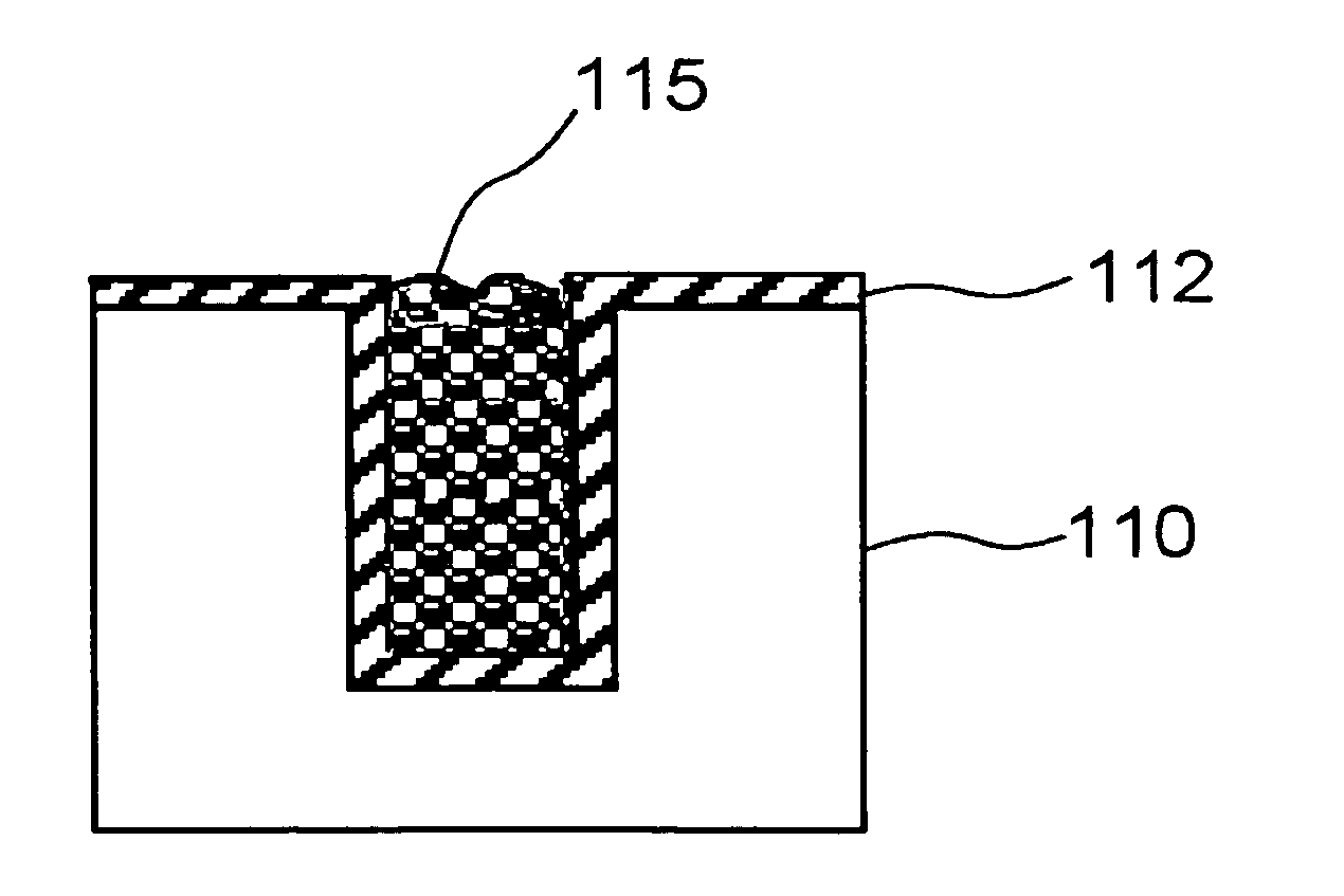
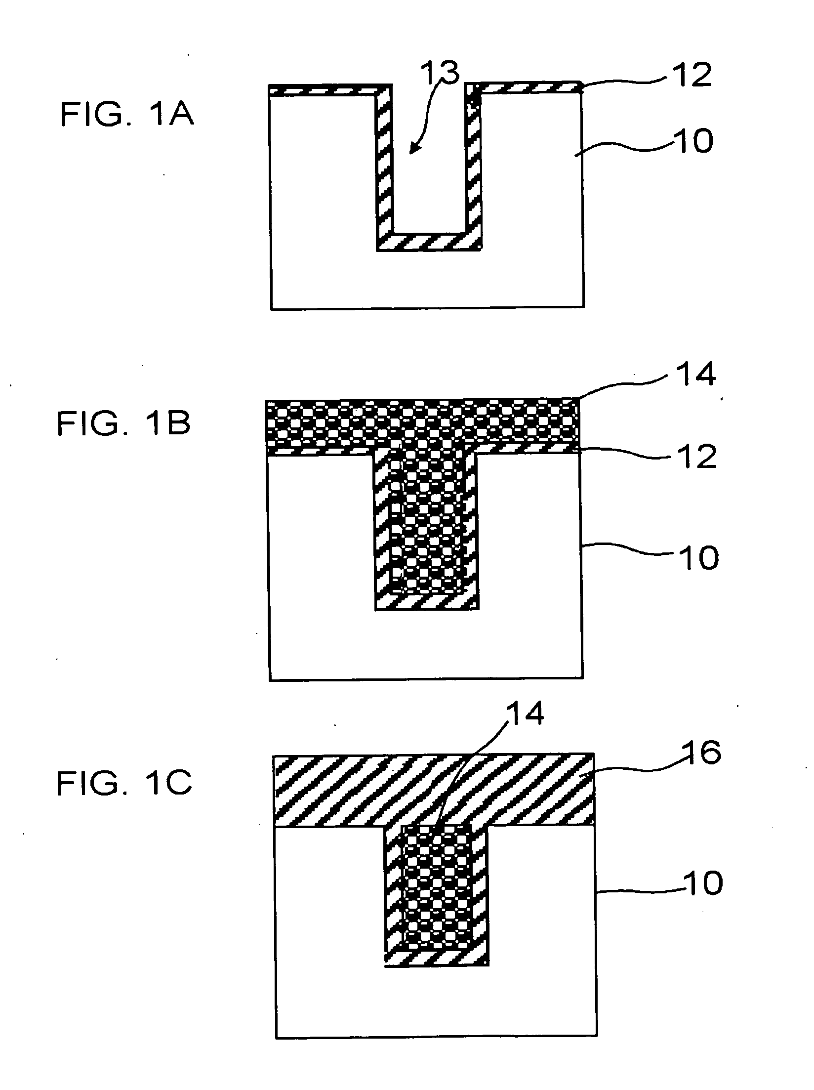
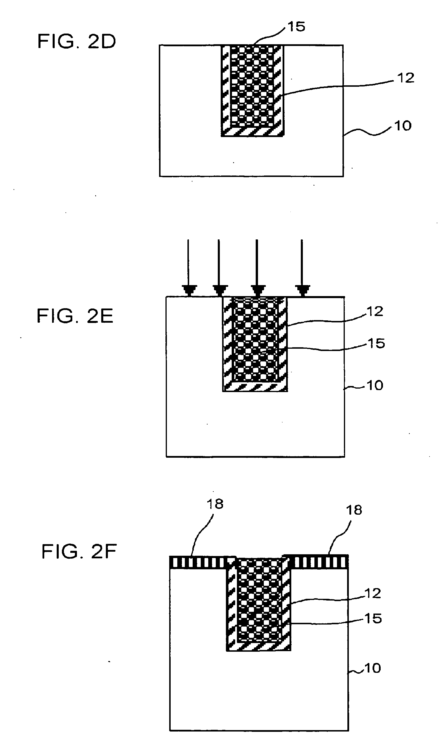
[0029] A method for manufacturing a semiconductor device according to the present embodiment comprises: forming a trench 13 in a silicon substrate 10; forming a first insulating film (first silicon oxide film 12) on a surface of the silicon substrate 10 including an interior wall of the trench 13 (FIG. 1A); forming a polysilicon film 14 which plugged in the trenc...


PUM


Abstract

A semiconductor device having an improved connecting reliability of an interconnect is presented via a simple and easy process, and further, a semiconductor device having a stable threshold voltage of a transistor that provide a stable electrical characteristic is also presented. A method for manufacturing a semiconductor device according to the present invention comprises: forming a trench in a silicon substrate; forming a first insulating film on a surface of said silicon substrate, said surface including an interior wall of said trench; forming a polysilicon film which plugged in said trench and covered on an entire surface of said silicon substrate; forming a second insulating film with oxidizing a portion of said polysilicon film disposed outside of said trench, and oxidizing a surface region of said silicon substrate located right under said first insulating film disposed outside of said trench and a surface region of said polysilicon film in said trench; and forming an embedded polysilicon layer with removing said second insulating film so that the surface of said silicon substrate is partially exposed and said polysilicon film is partially remained in said trench.

Description

[0001] This application is based on Japanese patent application Nos. 2005-120,319 and 2006-108626, the contents of which are incorporated hereinto by reference. BACKGROUND [0002] 1. Field of the Invention [0003] The present invention relates to a method for manufacturing a semiconductor device. [0004] 2. Related Art [0005] Conventional methods for manufacturing an embedded polysilicon layer typically includes a method described in, for example, Japanese Patent Laid-Open No. H06-314,739 (1994). The method for manufacturing the polysilicon layer described in Japanese Patent Laid-Open No. H06-314,739 is shown in FIGS. 6A to 6C and FIGS. 7D to 7F. [0006] First of all, a trench 113 is formed in a silicon substrate 110. Thereafter, a p-type diffusion layer (not shown) and an n-type diffusion layer (not shown) are formed in predetermined locations of the silicon substrate 110. Then, a silicon oxide film 112 is formed on surfaces of a silicon substrate 110 that includes an interior wall of ...

Claims


Application Information

Patent Timeline
IPC IPC(8): H01L21/76
CPCH01L29/66734H01L21/763
Inventor OHTANI, KINYA
Owner RENESAS ELECTRONICS CORP
Why Eureka
Try Eureka