Optical lithography correction process
a technology of optical lithography and correction process, applied in the field of optical lithography correction process, can solve the problems of increasing manufacturing costs, unable to provide any help in actual production, and unable to meet the requirements of the final microcircui
- Summary
- Abstract
- Description
- Claims
- Application Information
AI Technical Summary
Problems solved by technology
Method used
Image
Examples
Embodiment Construction
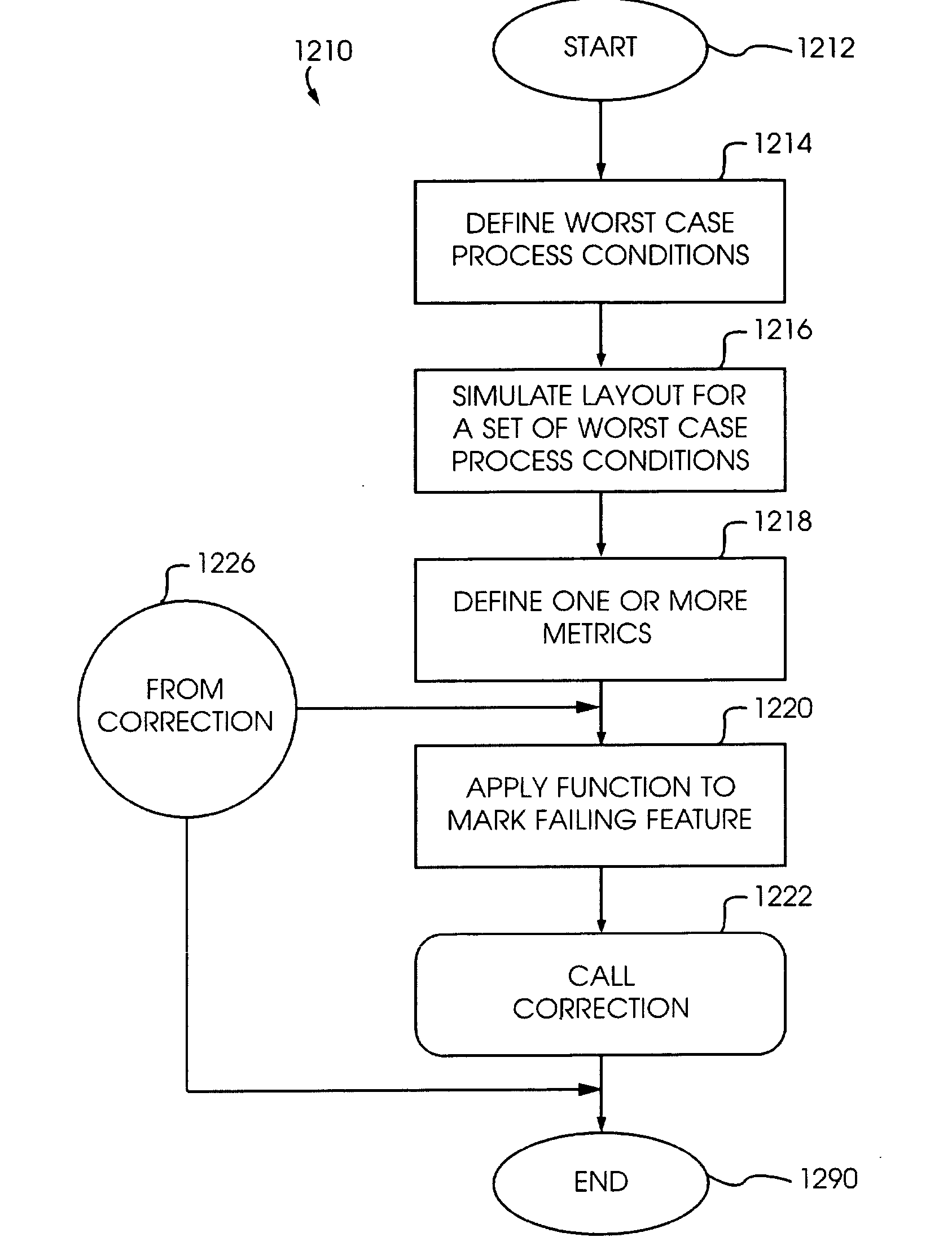
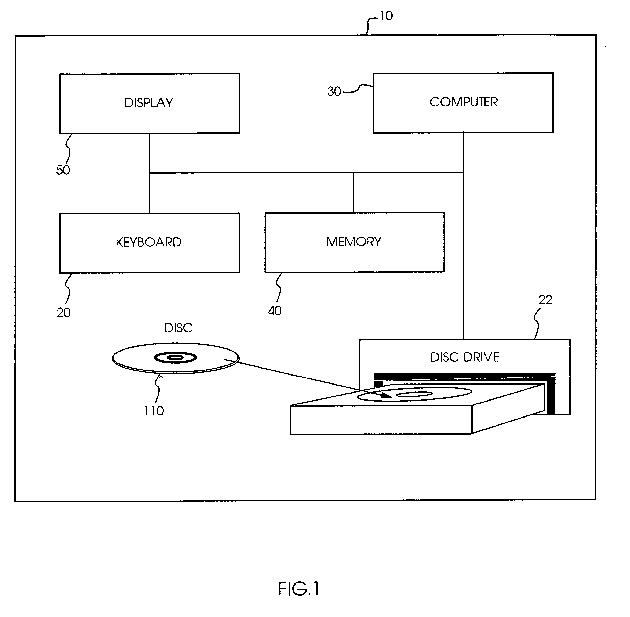
[0020] Referring now to the drawings and more particularly to FIGS. 1 and 12, there is illustrated a computer-aided design (CAD) system 10, which is constructed according to one of the preferred embodiments of the present invention. In this embodiment, the CAD system 10, through a computer readable program product 110, implements a resolution enhancement technique 1210 (FIG. 12) in an optical lithography process. More particularly, through an optical rule checking (ORC) process, the resolution enhancement technique 1210 verifies whether a distorted mask solution in fact creates the necessary effects to significantly reduce the risk of pattern failures in the printing process, and effectively increase the throughput of a nano-circuit production run when utilizing silicon wafer features having size dimensions significantly smaller than the wavelength of light. In this regard, the resolution enhancement technique 1210 characterizes the influence of individual ones of a plurality of wor...
PUM
 Abstract
Description
Claims
Application Information


