Plasma display panel

a technology of plasma display panel and display panel, which is applied in the direction of gas discharge vessel/container, electrode, gas-filled discharge tube, etc., can solve the problems of relative high discharge voltage and degraded and achieve the effect of improving the light efficiency of plasma display panel

Inactive Publication Date: 2006-10-26
SAMSUNG SDI CO LTD
View PDF16 Cites 9 Cited by
  • Summary
  • Abstract
  • Description
  • Claims
  • Application Information

AI Technical Summary

Benefits of technology

[0013] Accordingly, the present invention has been made to solve one or more of the above-mentioned problems occurring in the plasma display panel employing an opposed discharge scheme, and an object of the claimed invention is to provide a plasma display panel including an elect

Problems solved by technology

However, in the three-electrode type surface discharge scheme, since a distance between the scan electrode and the address electrode is short, a relatively high discharge voltage is required.
In this way, the plasma d

Method used


Image

  • Plasma display panel
  • Plasma display panel
  • Plasma display panel

Examples


first embodiment

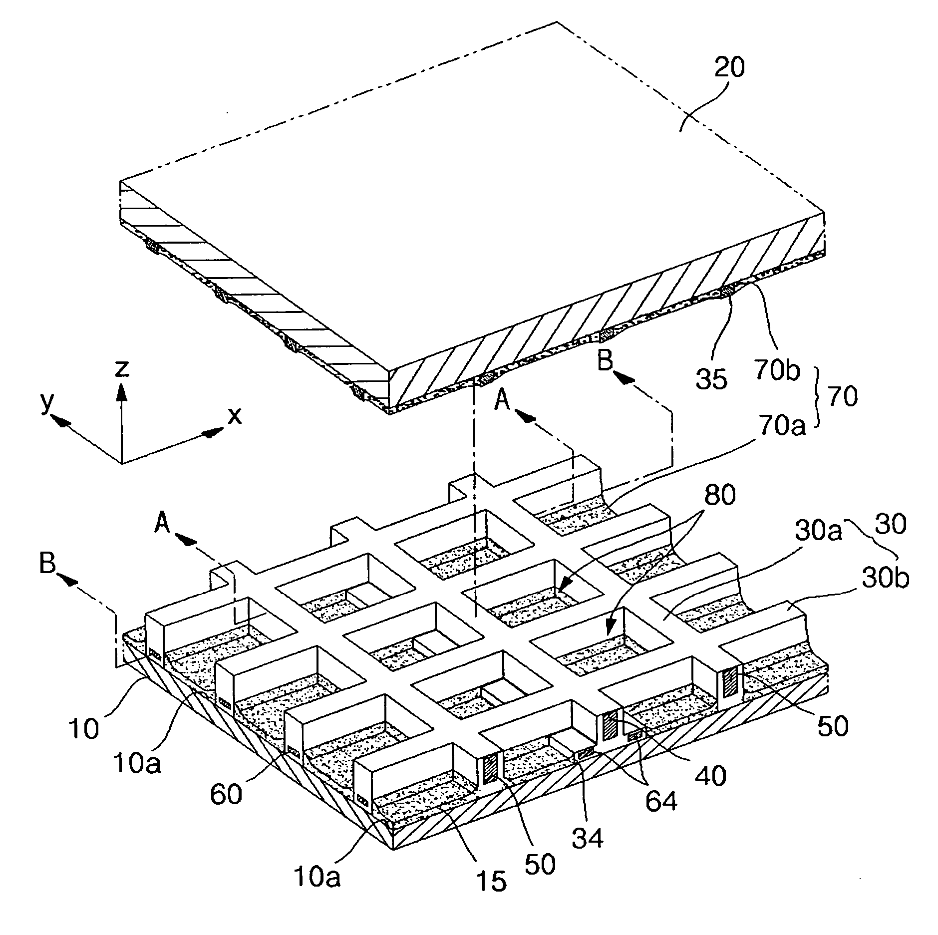
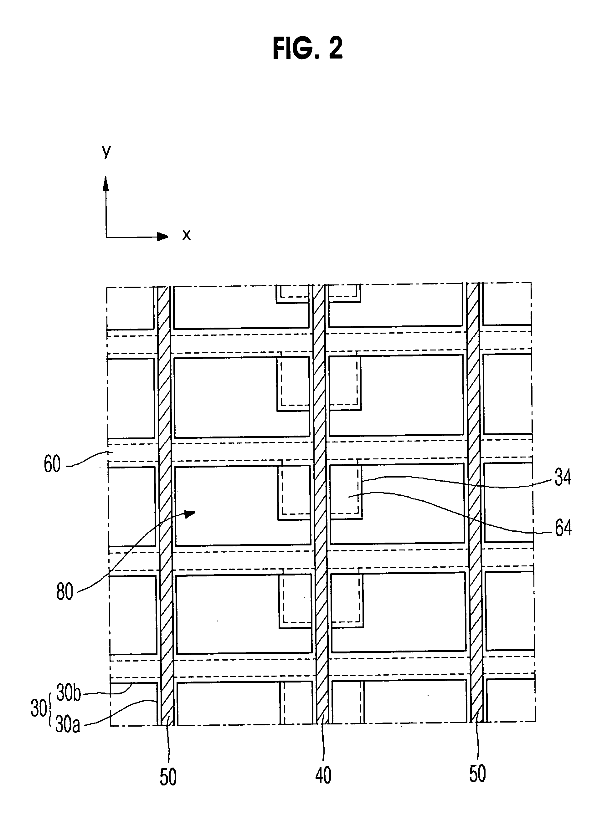
[0026]FIG. 1 is a partially exploded perspective view illustrating a plasma display panel according to the present invention, FIG. 2 is a horizontal sectional view taken along line A-A shown in FIG. 1, FIG. 3 is a horizontal sectional view taken along line B-B shown in FIG. 1, and FIG. 4 is a vertical sectional view of the plasma display panel shown in FIG. 1.

[0027] Referring to FIGS. 1 to 4, the plasma display panel according to the first embodiment of the present invention includes a first substrate (hereinafter, referred to as a rear substrate) 10, a second substrate (hereinafter, referred to as a front substrate) 20, barrier ribs 30, first electrodes 40 and second electrodes 50. The rear substrate 10 and the front substrate 20 face each other while forming a predetermined interval therebetween, and a plurality of discharge cells 80 are defined by means of the barrier ribs 30 in a space formed between the rear substrate 10 and the front substrate 20. The discharge cell 80 include...

second embodiment

[0048] Referring to FIG. 5, in the plasma display panel according to the present invention, an auxiliary electrode dielectric layer 134 surrounds the auxiliary address electrodes 64. In addition, the auxiliary electrode dielectric layer 134 is connected to other second barrier ribs 30b, which are located opposite the second barrier ribs 30b about the discharge cells 80. That is, the auxiliary electrode dielectric layer 134 is formed over the whole area of one side of the discharge cell 80. Thus, the internal structure of the discharge cell 80 may be simplified as compared with that of the discharge cell 80 shown in FIG. 1 so that the auxiliary electrode dielectric layer 134 can be easily formed. Since the auxiliary electrode dielectric layer 134 is an insulating layer, the auxiliary address electrodes 64 can be electrically disconnected from the other address electrodes 60, which are located opposite the auxiliary address electrodes 64 about the discharge cells 80.

[0049] Hereinafter...


PUM


Abstract

Disclosed is a plasma display panel. The plasma display panel includes an electrode structure in which an address electrode and a scan electrode generating an address discharge are aligned adjacent to each other such that an address voltage is constantly maintained at a relatively low level, thereby improving the light efficiency of the plasma display panel.

Description

CLAIM OF PRIORITY [0001] This application makes reference to, incorporates the same herein, and claims all benefits accruing under 35 U.S.C. § 119 from an application earlier filed in the Korean Intellectual Property Office on the 18th of Apr. 2005 and there duly assigned Ser. No. 10-2005-0032104. BACKGROUND OF THE INVENTION [0002] 1. Technical Field [0003] The present invention relates to a plasma display panel. More particularly, the present invention relates to a plasma display panel including an electrode structure in which an address electrode and a scan electrode generating an address discharge are aligned adjacent to each other such that an address voltage is constantly maintained at a relatively low level, thereby improving the light efficiency of the plasma display panel. [0004] 2. Description of the Prior Art [0005] A plasma display panel refers to a panel used in a plasma display device, which is a kind of flat display devices, for realizing an image using a visible ray e...

Claims


Application Information

Patent Timeline
IPC IPC(8): H01J17/49H01J11/12H01J11/14H01J11/16H01J11/22H01J11/24H01J11/26H01J11/32H01J11/34H01J11/36H01J11/38H01J11/42
CPCH01J11/16H01J2211/323H01J2211/265H01J11/26H01J11/28H01J11/38H01J11/42
Inventor HUR, MINCHOI, YOUNG-DO
Owner SAMSUNG SDI CO LTD
Why Eureka
Try Eureka