Integrated circuit and method of improving signal integrity

a technology of integrated circuits and integrated circuits, applied in the field of integrated circuits, can solve the problems of reducing flexibility, board space penalties, research and development set-up time costs, and the need for external switches, so as to improve the integrity of high-frequency parts, and improve the degree of design flexibility

Inactive Publication Date: 2006-10-26
AVAGO TECH WIRELESS IP SINGAPORE PTE
View PDF6 Cites 4 Cited by
  • Summary
  • Abstract
  • Description
  • Claims
  • Application Information

AI Technical Summary

Benefits of technology

[0020] According to a second aspect of the present invention, there is provided a use of an array of selectable impedances for an integrated circuit output stage, the use being to match an output impedance of the integrated circuit with an expected load so as to improve integrity of a high-frequency part of a broadband data signal.
[0021] The expected load may be defined at least in part by at least one piece-part of a circuit board for coupling to the integrated circuit. p According to a third aspect of the present invention, there is provided a method of improving integrity of a high-frequency part of a broadband data signal, the method comprising the step of: matching an impedance of an output stage of an integrated circuit to an expected load.
[0022] The selectable logic family output stage IC therefore provides a single IC capable of generating, in use, an output signal at a single terminal or pad having logic levels conforming to one of a number of selectable logic families. Printed Circuit Boards (PCBs) do not, therefore need to be provided with external switches to select a desired logic family for the output signal. The need to design the PCB to accommodate ICs having different pin-configurations is also obviated, as is the need to select and hardwire one of a number of output pads of a known IC to the PCB. Consequently, the IC of the present invention is well suited to a number of different applications using, if required, a single PCB design. It can therefore be seen that a greater degree of design flexibility is available to a designer of transceiver modules, resulting in further benefits in terms of the need for fewer components, savings in PCB space used, component costs and research and development setup time needed.
[0023] By sharing terminating resistors, parasitic loading effects are mitigated, permitting some output stage integrated circuits to be operated at frequencies of the order of GHz. Additionally, strategic positioning of the Field Effect Transistors (FETs) in the integrated circuit avoids deterioration of the output signals caused by loading effects in either PECL or CML modes, thereby enabling high-frequency operation.
[0024] It is also thus possible, using the programmable matching capacitor, to maintain the integrity, i.e. shape, of a PECL output signal. Additionally, the matching capacitors provide, for CML output signals, Electromagnetic Interference (EMI) filtering to maintain optimum system performance for various d ifferent data rate applications.

Problems solved by technology

A disadvantage of providing different output signals at respectively different output terminals is that selection of one of the number of output signals requires a switch external to the integrated circuit to switch a desired output signal onto the circuit board, or hardwiring of an output terminal, corresponding to the desired logic family, to the circuit board.
Unfortunately, the need for the external switch is accompanied by component costs, board space penalties and research and development set-up time costs.
The option of hardwiring the integrated circuit is at the cost of a reducing in flexibility.
However, the topology of the output stage cannot be changed easily without remanufacture, constituting a flexibility penalty.

Method used


Image

  • Integrated circuit and method of improving signal integrity
  • Integrated circuit and method of improving signal integrity
  • Integrated circuit and method of improving signal integrity

Examples


Embodiment Construction

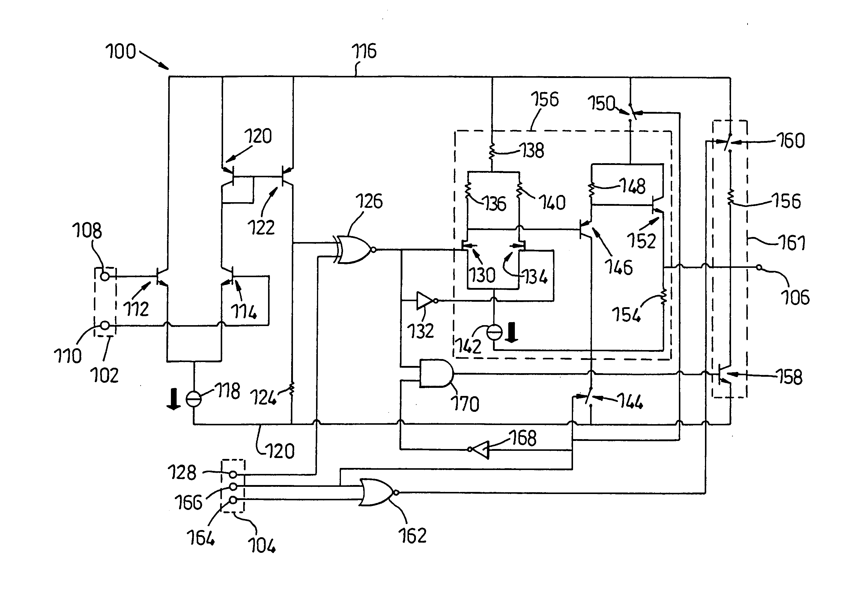
[0029] Referring to FIG. 1, a selectable logic family output stage IC 100 comprises a first input 102, a second input 104 and an output 106. The first input 102 comprises a first differential input terminal 108 and a second differential input terminal 110, the first differential input terminal 108 being coupled to a base terminal of a first npn bipolar transistor 112 and the second differential input terminal 110 being coupled to a base terminal of a second npn bipolar transistor 114.

[0030] A collector terminal of the first npn transistor 112 is coupled to, in this example, a positive power rail 116 maintained at Vcc volts by a power supply (not shown). An emitter terminal of the first npn transistor 112 and an emitter terminal of the second npn transistor 114 are coupled to a first terminal of a constant current source 118, a second terminal of the current source 118 being coupled to a ground rail 120.

[0031] A collector terminal of the second npn transistor 114 is coupled to a co...


PUM


Abstract

An Integrated Circuits (ICs) comprising a first output stage circuit and a second output stage circuit that share common input terminals and an output terminal of the first and second output stage circuits being selectably coupled between the input terminals and the output terminal in preference to the other.

Description

CROSS-REFERENCED APPLICATIONS [0001] This application is a continuation application of U.S. patent application Ser. No. 10 / 910,067, filed on Aug. 3, 2004.FIELD OF THE INVENTION [0002] The present invention relates to an integrated circuit of the type capable of generating output signals having logic levels substantially conforming to those of a first logic family, for example Positive Emitter-Coupled Logic (PECL), Current Mode Logic (CML), or Transistor-Transistor Logic (TTL). The present invention also relates to a method of improving signal integrity, for example for signals generated by the above-mentioned integrated circuit. DISCUSSION OF THE BACKGROUND ART [0003] A fibre-optic transceiver module typically comprises an output stage circuit for an interface between the transceiver module and a circuit board for receiving the transceiver module. The output stage circuit is usually manufactured as part of an integrated circuit for connection to the circuit board, the integrated cir...

Claims


Application Information

Patent Timeline
Patent Type & Authority Applications(United States)
IPC IPC(8): H03K19/003H03K19/00H03K19/0175H04L25/02
CPCH03K19/0005H03K19/017581H04L25/0282H04L25/028H04L25/0278H04L25/026H04L25/085
Inventor RITCHIE, CHARLES GRAEMESEIFU, FESSEHA TESSERA
Owner AVAGO TECH WIRELESS IP SINGAPORE PTE
Why Eureka
Try Eureka