Method of manufacturing a semiconductor device

a manufacturing method and semiconductor technology, applied in semiconductor devices, semiconductor/solid-state device details, electrical devices, etc., can solve the problems of deteriorating mask alignment accuracy, and achieve the effect of preventing cracking or chipping in the semiconductor device, and reducing the damage to the semiconductor chip in die bonding

Inactive Publication Date: 2006-10-26
RENESAS ELECTRONICS CORP
View PDF4 Cites 30 Cited by
  • Summary
  • Abstract
  • Description
  • Claims
  • Application Information

AI Technical Summary

Benefits of technology

[0024] Since there is provided a lead frame wherein the thickness of a tab-side end portion of a metal plating for wire connection formed on each suspending lead is smaller than the thickness of a metal plating for wire connection formed on each lead, and thereafter a semiconductor chip is mounted onto a tab, the metal plating on each suspending lead is crushed and ther

Problems solved by technology

In this case, the mask alignment accuracy is deteriorated as the

Method used


Image

  • Method of manufacturing a semiconductor device
  • Method of manufacturing a semiconductor device
  • Method of manufacturing a semiconductor device

Examples


first embodiment

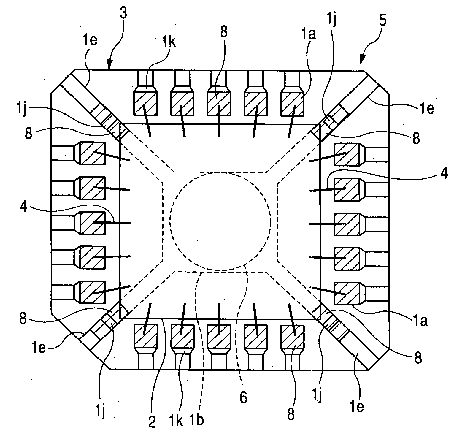
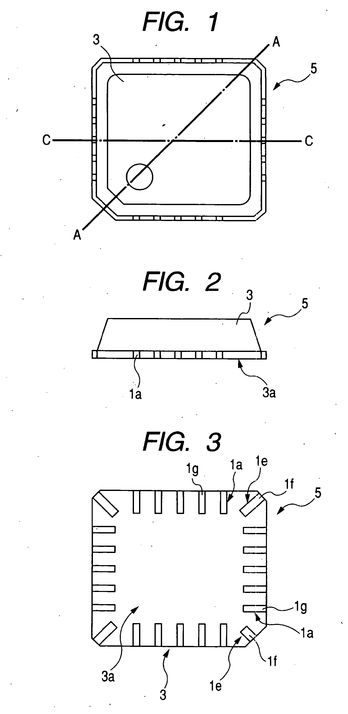
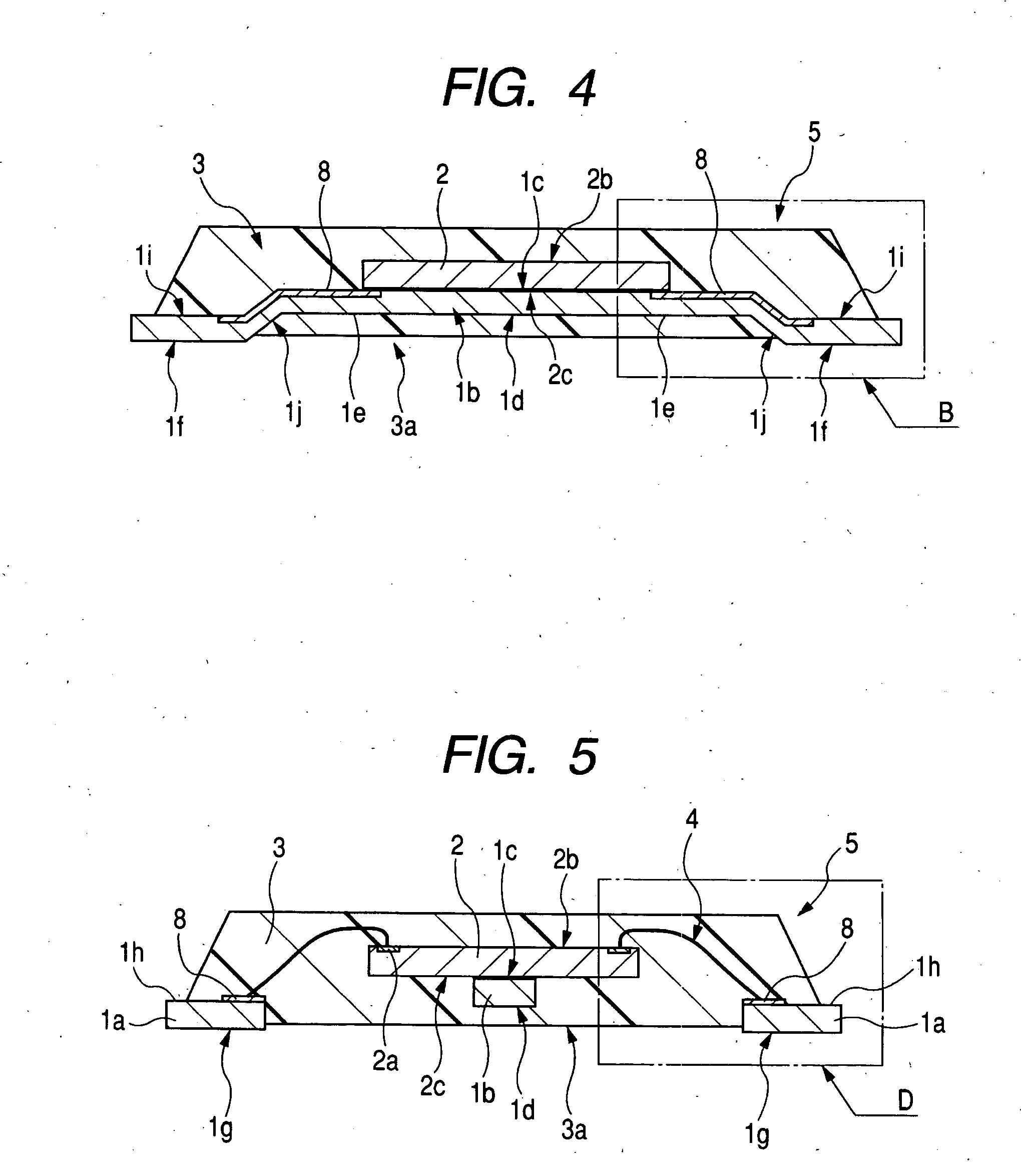
[0056]FIG. 1 is a plan view showing an example of the structure of a semiconductor device according to a first embodiment of the present invention, FIG. 2 is a side view thereof, FIG. 3 is a back view thereof, FIG. 4 is a sectional view showing the structure of a section cut along line A-A in FIG. 1, and FIG. 5 is a sectional view showing the structure of a section cut along line C-C in FIG. 1. FIG. 6 is a partial enlarged sectional view showing on a larger scale a structural example of portion B in FIG. 4, FIG. 7 is a partial enlarged sectional view showing on a larger scale a structural example of portion D in FIG. 5, and FIG. 8 is a plan view showing an example of an internal structure of the semiconductor device of FIG. 1 as seen through a sealing body. FIG. 9 comprises plan views and sectional views, showing an example of a method for forming a metal plating onto a lead frame used in assembling the semiconductor device of FIG. 1, FIG. 10 is a partial sectional view showing an e...

second embodiment

[0118]FIG. 20 is a pan view-showing a structural example of a semiconductor device according to a second embodiment of the present invention, FIG. 21 is a side view thereof, FIG. 22 is a back view thereof, FIG. 23 is a sectional view showing the structure of a section taken along line A-A in FIG. 20, and FIG. 24 is a sectional view showing the structure of a section taken along line C-C in FIG. 20.

[0119] The semiconductor device of this second embodiment shown in FIGS. 20 to 24 is a resin-sealed type QFP (Quad Flat Package) 11 wherein plural outer leads 1p serving as external terminals are projected from four side faces of a sealing body 3 formed of resin.

[0120] The QFP 11 comprises a tab 1b connected to a semiconductor chip 2, suspending leads 1e which support the tab 1b, plural inner leads in arranged around the semiconductor chip 2, wires 4 for electric connection between pads 2a of the semiconductor chip 2 and the inner leads in, outer leads 1p connected integrally with the in...


PUM


Abstract

According to the method of manufacturing a semiconductor device, a lead frame is provided wherein the thickness of a tab-side end portion of a silver plating for wire connection formed on each suspending lead 1e is smaller than that of a silver plating formed on each lead. Thereafter, a semiconductor chip is mounted onto a tab. In this case, since the entire surface of the silver plating on the suspending lead 1e is in a crushed state, it is possible to prevent contact of the semiconductor chip with the silver plating when mounting the chip onto the tab. Consequently, in a die bonding process, the semiconductor chip can slide on the tab without contacting the silver plating and thereby making it possible to diminish damage to the semiconductor chip when mounted onto the tab and hence to possibly prevent cracking or chipping of the chip when assembling the semiconductor device.

Description

BACKGROUND OF THE INVENTION [0001] The present invention relates to a semiconductor device manufacturing technique and particularly a technique applicable effectively to the manufacture of a semiconductor device having plated suspending leads. [0002] A QFN (Quad Flat Non-leaded Package) type semiconductor device comprises a tab which supports a semiconductor chip, a sealing portion formed by sealing the semiconductor chip with resin, tab suspending leads for supporting the tab, and a plurality of leads exposed to peripheral edge portions of a back surface of the sealing portion, the tab being a small tab and sealed with the sealing resin (see, for example, Patent Literature 1). [0003] [Patent Literature 1][0004] International Publication WO 01 / 003186 (FIG. 40) SUMMARY OF THE INVENTION [0005] In assembling such a semiconductor device as a QFN type semiconductor device there is used a lead frame having leads plated with silver for wire connection. The silver plating for the leads of t...

Claims


Application Information

Patent Timeline
IPC IPC(8): H01L21/00
CPCH01L21/4842H01L23/49551H01L2224/49171H01L2924/014H01L2924/01006H01L2924/01005H01L2924/00014H01L2224/32245H01L2924/01082H01L2924/01079H01L2924/01078H01L2924/01057H01L2924/01047H01L2924/01046H01L23/49582H01L24/45H01L24/48H01L24/85H01L2224/45144H01L2224/48091H01L2224/48247H01L2224/73265H01L2224/85439H01L2224/85464H01L2924/01004H01L2924/01029H01L2924/01033H01L2224/78H01L2924/00012H01L2924/00H01L24/49H01L24/73H01L2224/48639H01L2224/48664H01L2924/181H01L23/12H01L23/50
Inventor AMANO, KENJIHASEBE, HAJIME
Owner RENESAS ELECTRONICS CORP
Why Eureka
Try Eureka