Multi-channel semiconductor device and method of manufacturing the same

a semiconductor and multi-channel technology, applied in semiconductor devices, building types, construction, etc., can solve the problems of increasing the capacitance of the source/drain junction, increasing the leakage current, and damaging the active layer

Inactive Publication Date: 2006-10-26
SAMSUNG ELECTRONICS CO LTD
View PDF4 Cites 178 Cited by
  • Summary
  • Abstract
  • Description
  • Claims
  • Application Information

AI Technical Summary

Benefits of technology

[0037]FIGS. 5A and 5B are respectively a characteristic curve of the C...

Problems solved by technology

The reduced length of the channel causes a short channel effect, thereby increasing leakage current.
Moreover, an increase in the number of channels results in the increase of a source/drain junction capacitance.
This oxidation process m...

Method used


Image

  • Multi-channel semiconductor device and method of manufacturing the same
  • Multi-channel semiconductor device and method of manufacturing the same
  • Multi-channel semiconductor device and method of manufacturing the same

Examples


Embodiment Construction

[0038] The present invention will now be described more fully with reference to the accompanying drawings, in which exemplary embodiments of the invention are shown. It will be understood that when a layer is referred to as being “on” another layer or substrate, it can be directly on the other layer or substrate, or intervening layers may also be present.

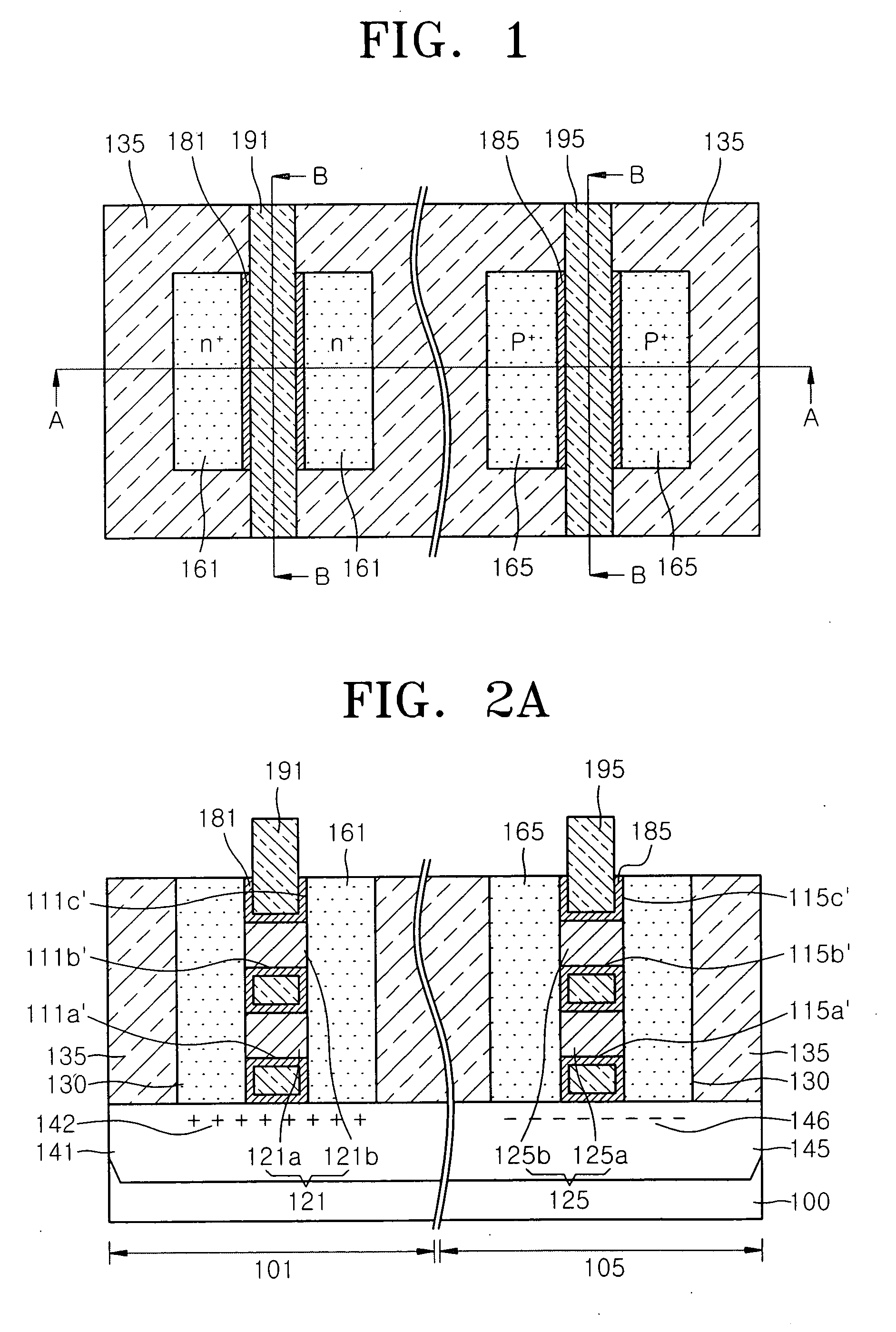
[0039]FIG. 1 is a plan view of a CMOS transistor according to an embodiment of the present invention. In FIG. 1, the left portion of the drawing corresponds to an NMOS transistor and the right portion of the drawing corresponds to a PMOS transistor.

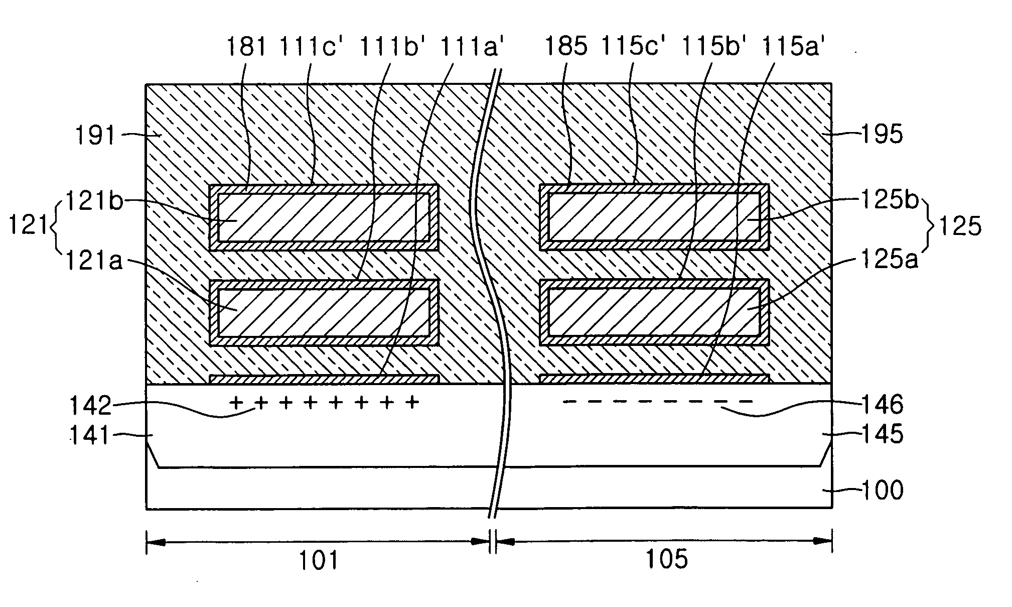
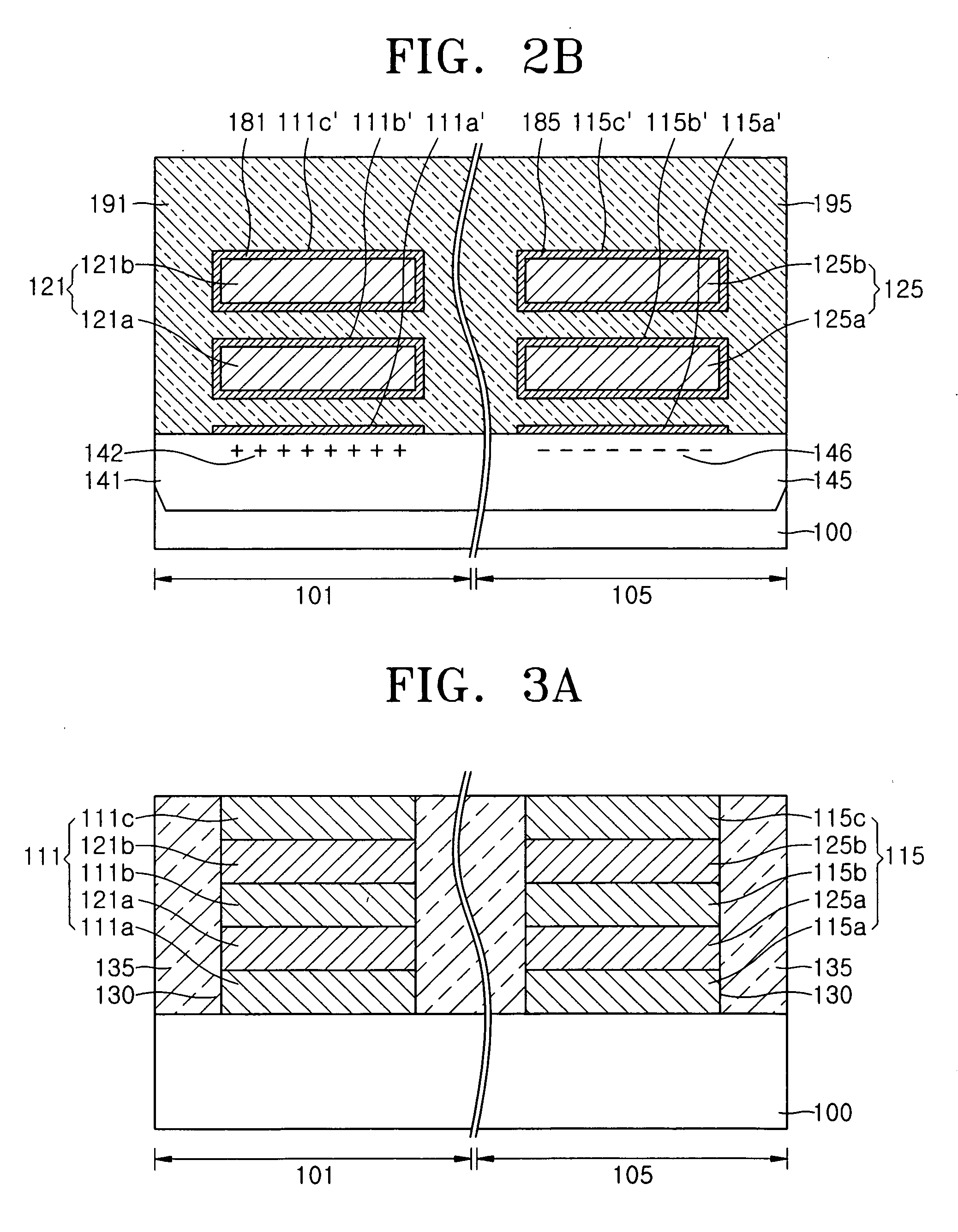
[0040]FIG. 2A is a sectional view taken along line A-A of FIG. 1, and FIG. 2B is a sectional view taken along line B-B of FIG. 1. In FIGS. 2A and 2B, the left portion of the drawings corresponds to an NMOS transistor and the right portion of the drawings corresponds to a PMOS transistor.

[0041] Referring to FIGS. 1, 2A and 2B, a semiconductor substrate 100 includes a first transistor re...


PUM


Abstract

Provided are a multi-channel semiconductor device and a method for manufacturing the semiconductor device through a simplified process. A sacrificial layer and a channel layer are alternately stacked on a semiconductor substrate. Thereafter, the sacrificial layer and the channel layer are etched to form a separated active pattern, and a device isolation layer is formed to cover sidewalls of the active pattern. Dopant ions are implanted into the entire semiconductor substrate, thereby forming a channel separation region under the active pattern. A portion of the active pattern is etched to separate the active pattern from a pair of facing sidewalls of the device separation layer, thereby forming a channel pattern having a pair of first exposed sidewalls. Source/drain semiconductor layers are formed on the first sidewalls of the channel pattern, and a part of the device isolation layer is removed to expose a pair of second sidewalls of the channel pattern contacting with the device separation layer. Thereafter, the sacrificial layer included in the channel pattern is remove, and a conductive layer for a gate electrode is formed to cover the channel layer exposed by the removing of the sacrificial layer.

Description

CROSS-REFERENCE TO RELATED PATENT APPLICATION [0001] This application claims the benefit of Korean Patent Application No. 10-2005-0033200, filed on Apr. 21, 2005, in the Korean Intellectual Property Office, the contents of which are incorporated herein in their entirety by reference. BACKGROUND OF THE INVENTION [0002] 1. Field of the Invention [0003] The present invention relates to a semiconductor device, and more particularly, to a multi-channel CMOS transistor and a method of manufacturing the CMOS transistor through a simplified process. [0004] 2. Description of the Related Art [0005] With the high integration of a semiconductor device, an active region of the semiconductor device is reduced in size and thus a channel of a MOS transistor formed in the active region is reduced in length. The reduced length of the channel causes a short channel effect, thereby increasing leakage current. Also, as the size and a driving voltage of the MOS transistor are reduced, its output current ...

Claims


Application Information

Patent Timeline
IPC IPC(8): H01L21/336
CPCH01L29/42392H01L29/78645H01L29/785H01L29/66795E04H17/04E04H17/08
Inventor LEE, SUNG-YOUNGYUN, EUN-JUNG
Owner SAMSUNG ELECTRONICS CO LTD
Why Eureka
Try Eureka