Clock control circuit

a control circuit and clock technology, applied in the direction of generating/distributing signals, instruments, computing, etc., can solve the problems of large power consumption, difficult layout, holding circuits, etc., and achieve the effect of reducing the intensity of noise, reducing the influence, and reducing the increase of power consumption

Inactive Publication Date: 2006-10-26
LAPIS SEMICON CO LTD
View PDF1 Cites 12 Cited by
  • Summary
  • Abstract
  • Description
  • Claims
  • Application Information

AI Technical Summary

Benefits of technology

[0011] It is an object of the present invention to provide a clock control circuit which is capable of facilitating the switching of frequency and timing, and selecting a clock signal which entails less operation noise without requiring a fast reference clock signal.
[0015] Accordingly, the input / output circuit which performs an input / output operation based on the master clock signal, the processor which operates based on the bus clock signal, and the like operate at dispersed timings, thus producing such effects as a reduction in the intensity of noise due to operations synchronized to the clocks, and a reduction in the influence of malfunctions due to the noise.
[0016] Also, since a fast reference clock signal is not required, an increase in power consumption can be restrained. Further, since only one type of bus clock signal is supplied to the processor and the like, no need exists for a plurality of clock supply paths or a circuit for switching the paths, thus making it possible to simplify the circuit configuration.
[0017] The clock control circuit further comprises a first selector for selecting one of the output signal of the logical OR gate and the multiplied signal in accordance with a first selection signal and outputting the selected one as a multiplied bus clock signal, and a second selector for selecting one of the divided clock signal and the multiplied bus clock signal in accordance with a second selection signal, and outputting the selected one as the reference bus clock signal. In this way, since a multiplied clock signal can be selected from clock signals having four different timings, it is possible to readily select a clock signal associated with a timing at which malfunctions are less likely to occur. Further, by providing a resister for setting a division value, a multiplication value, a selection signal and the like, an optimal state can be set by a program.

Problems solved by technology

However, the data holding circuit has the following problems.
(1) The reference clock signal required by the data holding circuit is fast as compared with the rates of the data signals, resulting in larger power consumption.
(2) A plurality of clock supply paths are required, leading to difficulties in the layout due to a correction of the clock signals for skew.
(3) When the plurality of clock supply paths are switched, a circuit configuration therefor is complicated and large in scale.

Method used


Image

  • Clock control circuit
  • Clock control circuit
  • Clock control circuit

Examples


Embodiment Construction

[0025] In the following, embodiments of the present invention will be described in detail with reference to the drawings.

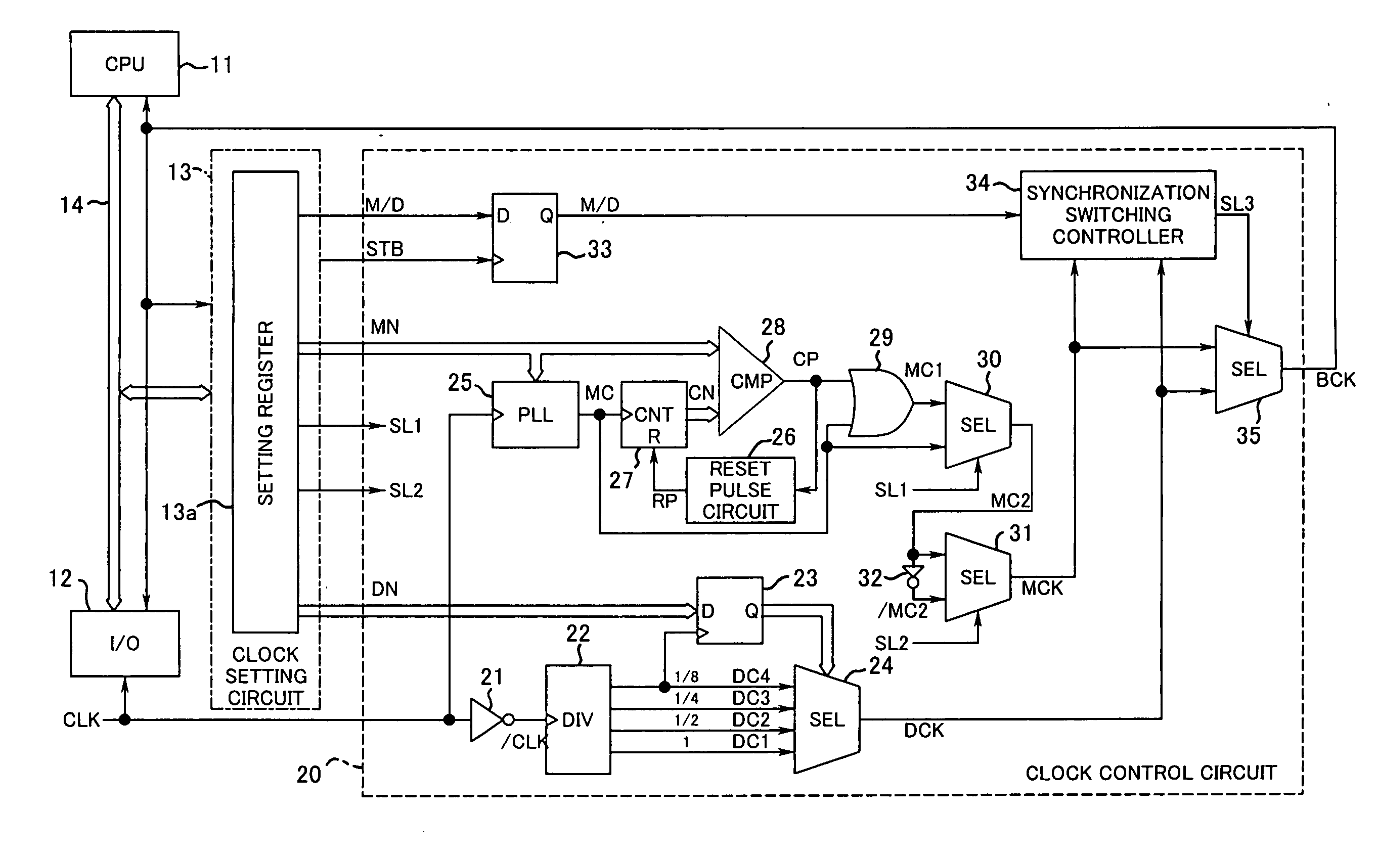
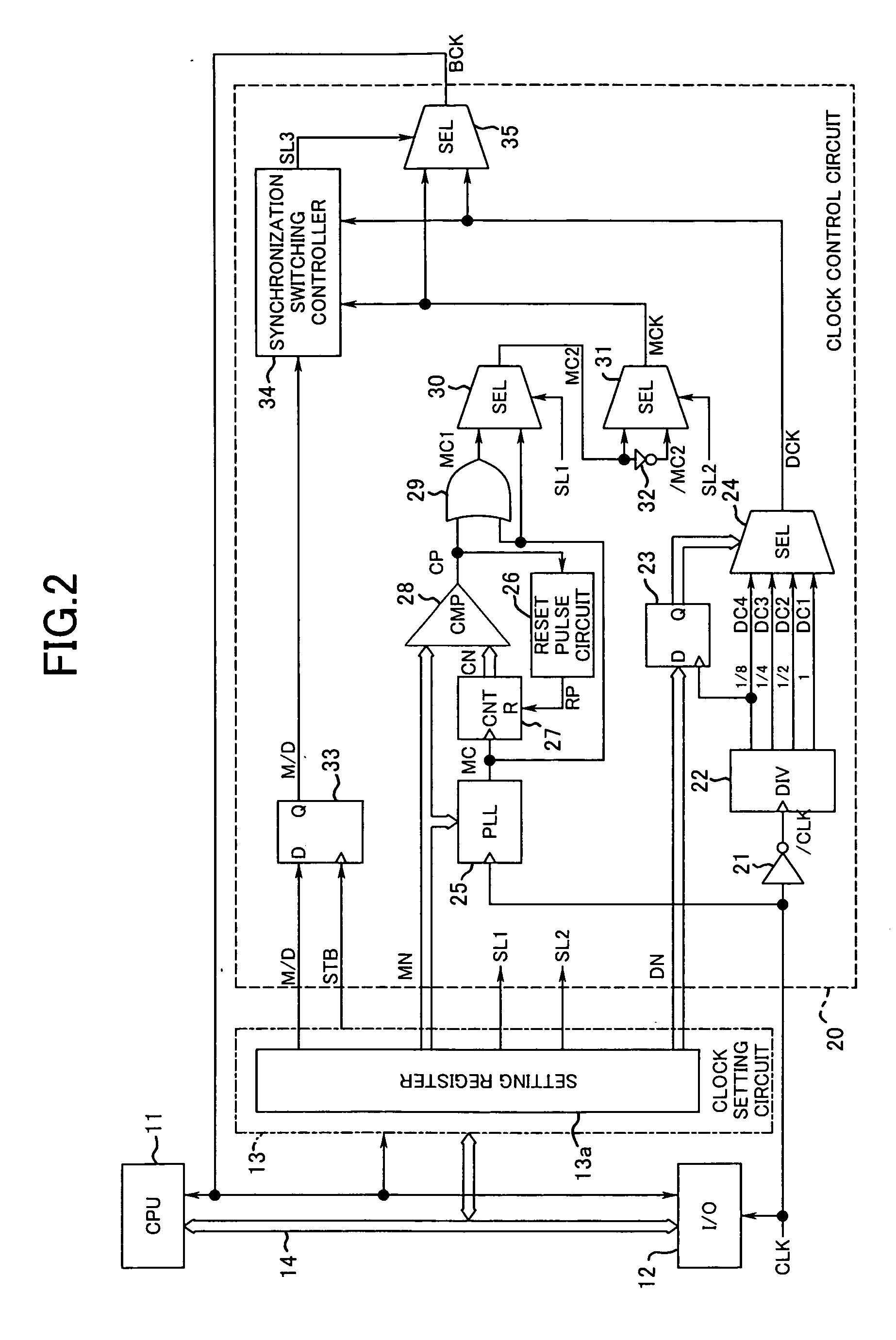
[0026]FIG. 2 is a schematic diagram of a clock control circuit showing an embodiment of the present invention. The clock control circuit 20 is built in a semiconductor integrated circuit, and generates a bus clock signal BCK for use within the semiconductor integrated circuit based on an external master clock CLK.

[0027] The semiconductor integrated circuit comprises, other than the clock control circuit 20, a processor (CPU) 11 for generally controlling the semiconductor integrated circuit in accordance with a program stored in a memory or the like, not shown; an input / output circuit (I / O) 12 for performing input / output operations with an external device (not shown); a clock setting circuit 13 for setting a clock for the clock control circuit 20; and the like. The processor 11, input / output circuit 12, clock setting circuit 13 and the like are interconnected thr...


PUM


Abstract

A clock control circuit including a divider unit for dividing a master clock signal at a falling timing of the same to generate a divided clock signal, a multiplier unit for multiplying the master signal by n at a rising timing of the same, and thinning out an n-th clock pulse to generate a multiplied clock signal, and a selector unit for selecting a bus clock signal from multiplied clock signals at a variety of timings, derived from the multiplied clock signal, and the divided clock signal in accordance with a selection signal, and supplying the selected signal to a processor.

Description

BACKGROUND OF THE INVENTION [0001] 1. Field of the Invention [0002] The present invention relates to a clock control circuit for generating a plurality of clock signals in a semiconductor integrated circuit. [0003] 2. Description of the Related Background Art [0004]FIG. 1 is a schematic diagram of a conventional data holding circuit shown in Japanese Patent Application Kokai No. 2002-215570. The data holding circuit comprises: a D-latch circuit 1 for holding and outputting a data signal D1i at a rising edge of a clock signal CK1; a D-latch circuit 2 for holding and outputting a data signal D2i at a falling edge of the clock signal CK1; a D-latch circuit 3 for holding and outputting a data signal D3i at a rising edge of a clock signal CK2; and a D-latch circuit 4 for holding and outputting a data signal D4i at a falling edge of the clock signal CK2. The signals held in these D-latch circuits 1-4 are output as data signals D1-D4, respectively, through buffers B1-B4. [0005] On the othe...

Claims


Application Information

Patent Timeline
Patent Type & Authority Applications(United States)
IPC IPC(8): G06F1/00
CPCG06F1/06
Inventor HANAMORI, HIROYUKI
Owner LAPIS SEMICON CO LTD
Why Eureka
Try Eureka