Built-in self-testing of multilevel signal interfaces

a multi-level signal and interface technology, applied in the field of multi-level digital signaling, can solve the problems of reducing the ability of receiving devices to distinguish binary signals, dividing signals into smaller levels for multi-pam, and affecting the implementation of multi-pam,

Inactive Publication Date: 2006-10-26
RAMBUS INC
View PDF39 Cites 15 Cited by
  • Summary
  • Abstract
  • Description
  • Claims
  • Application Information

AI Technical Summary

Benefits of technology

[0007] Error detection mechanisms for signal interfaces are disclosed, including built-in self-test (BIST) mechanisms for testing multilevel signal interfaces. The error detection mechanisms may be provided in an integrated circuit (IC) chip that contains at least one of the signal interfaces, or may be coupled to the interfaces on a printed circuit board (PCB). BIST mechanisms may include, for example, test signal generators and mechanisms for d

Problems solved by technology

At higher frequencies, however, receiving devices may have a reduced ability to distinguish binary signals, so that dividing signals into smaller levels for multi-PAM is problematic.
Multi-PAM may also be more difficult to implement in multi-drop bus systems (i.e., buses shared by multiple processing mechanisms), since the lower signal-to-noise ratio for such syste

Method used


Image

  • Built-in self-testing of multilevel signal interfaces
  • Built-in self-testing of multilevel signal interfaces
  • Built-in self-testing of multilevel signal interfaces

Examples


Embodiment Construction

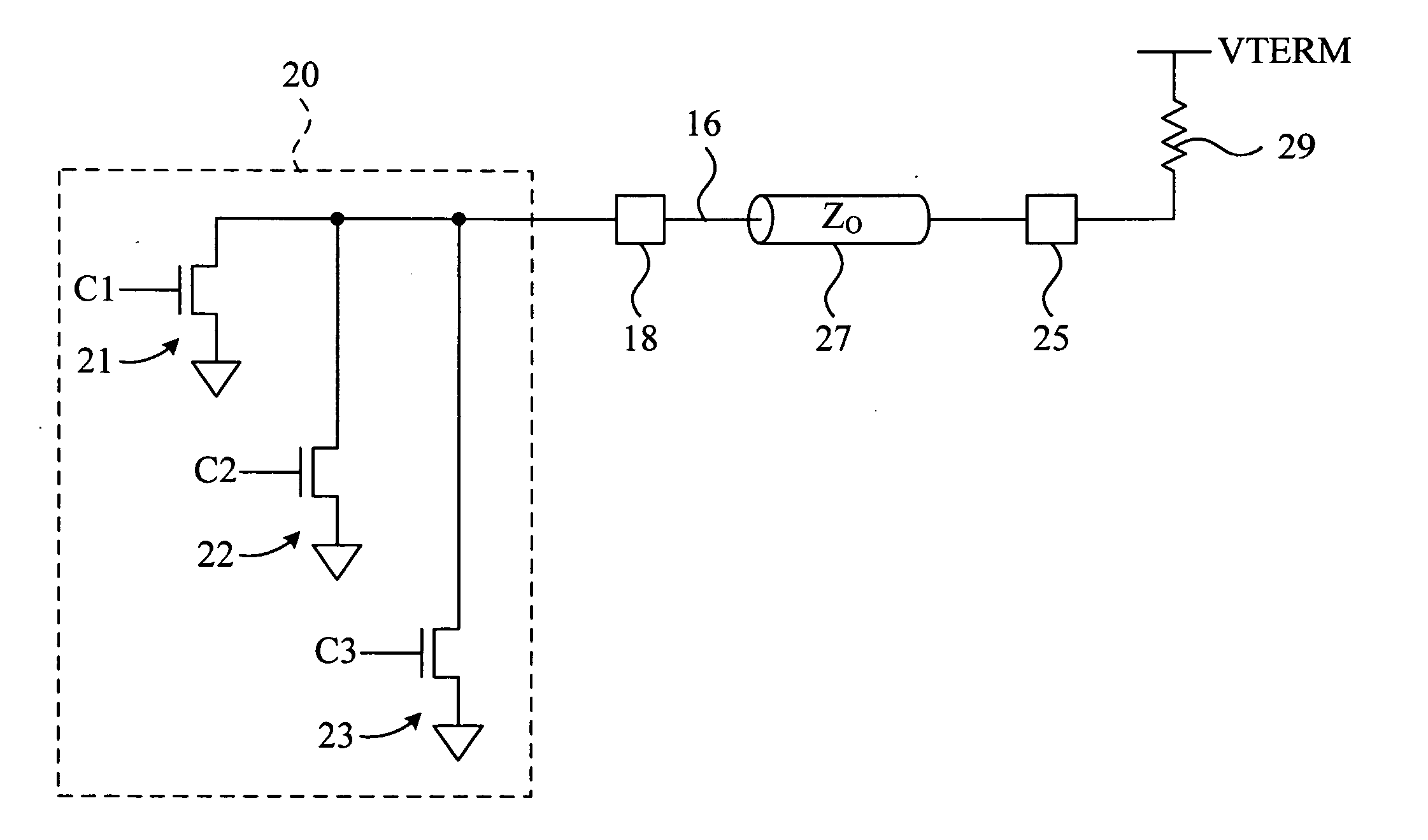
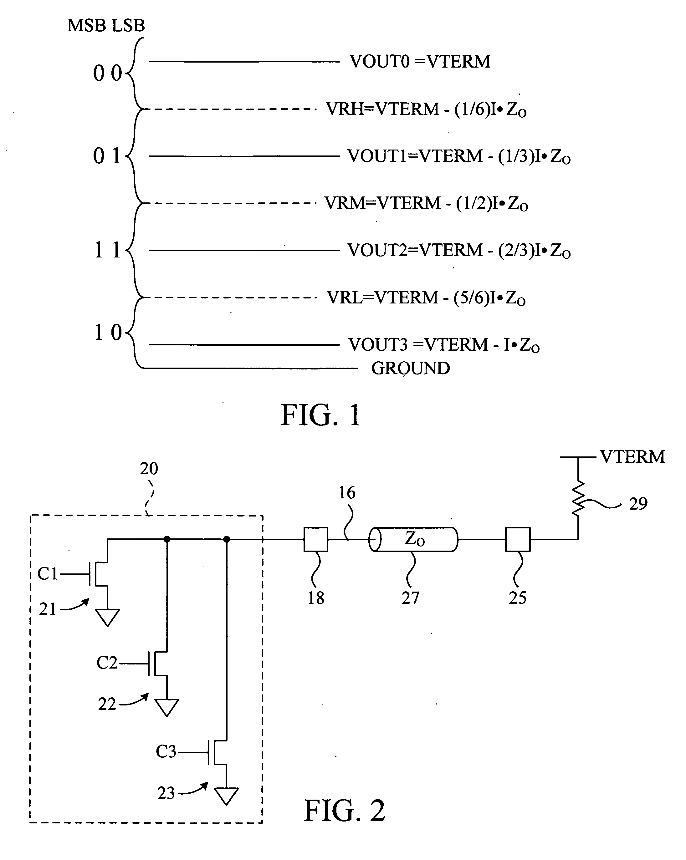
[0023]FIG. 1 shows a multilevel signal system having four logical states corresponding to four distinct voltage levels, VOUT0, VOUT1, VOUT2 and VOUT3. The voltage levels in this example are all positive relative to ground, and range as high as VTERM. VOUT0 is defined to be above VREFH, VOUT1 is defined to be between VREFM and VREFH, VOUT2 is defined to be between VREFL and VREFM, and VOUT3 is defined to be less than VREFL. VOUT0 corresponds to logical state 00, VOUT1 corresponds to logical state 01, VOUT2 corresponds to logical state 11, and VOUT3 corresponds to logical state 10. An example of the 4-PAM system described above has been implemented for a memory system interface having VOUT0=1.80V, VOUT1=1.533V, VOUT2=1.266V and VOUT3=1.00V. Although four logical states are illustrated in this example, a multilevel signal system may have more or less logical states, with at least two reference levels serving as boundaries between the states.

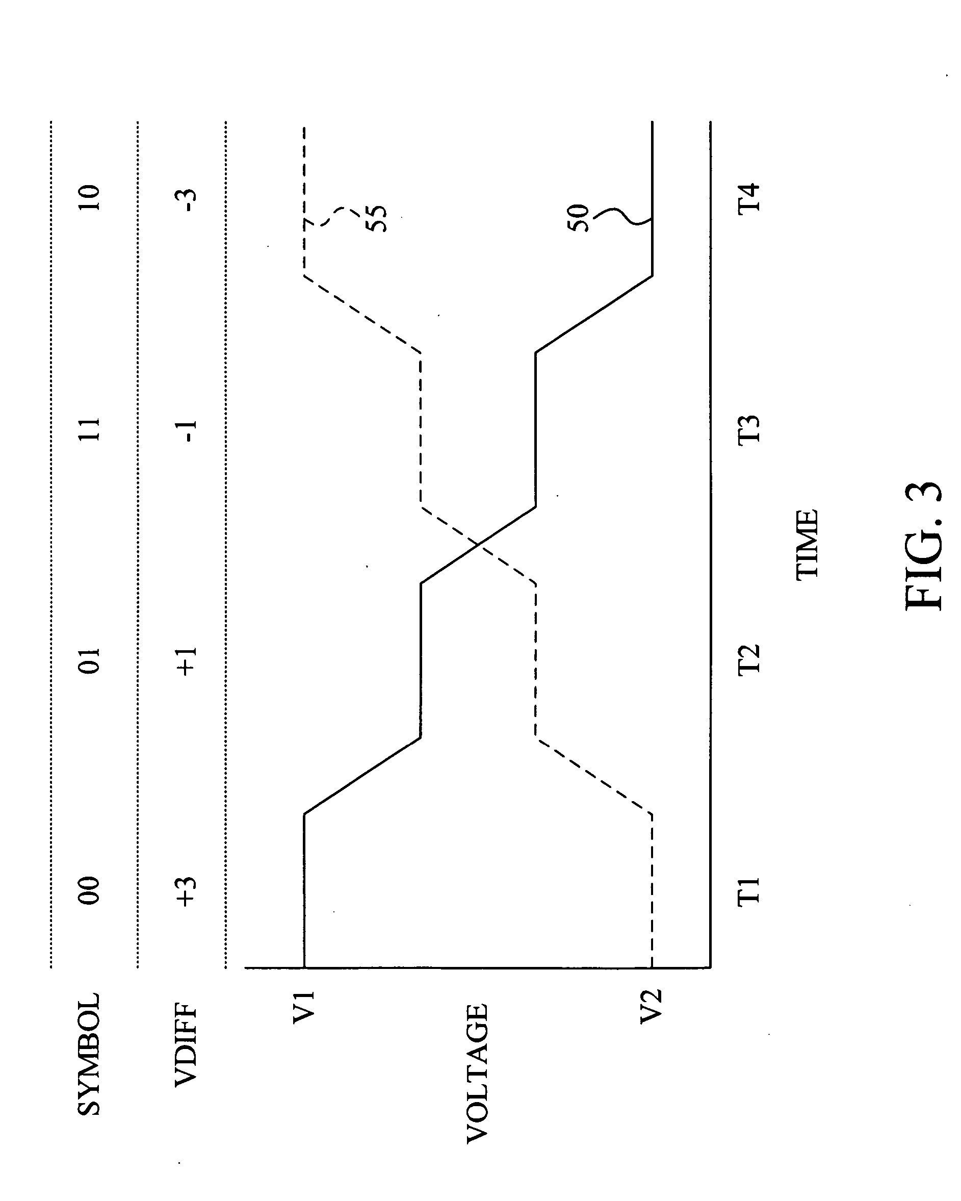
[0024] A first bit of each logical state is ...


PUM


Abstract

Error detection mechanisms for signal interfaces, including built-in self-test (BIST) mechanisms for testing multilevel signal interfaces. The error detection mechanisms are provided in an integrated circuit (IC) chip that contains at least one of the signal interfaces or are coupled to the interfaces on a printed circuit board (PCB). BIST mechanisms may include, for example, test signal generators and mechanisms for determining whether the test signals generated are accurately transmitted and received by the interface. The BIST mechanisms may check a single input/output interface, a group of interfaces or may operate with a master device that tests a plurality of interfaces by sending test signals for storage by and retrieval from one or more slave memory devices. The error detection mechanisms test memory circuits designed to communicate according to multi-PAM signals over printed circuit boards.

Description

[0001] This application claims the benefit under 35 U.S.C. §120 of U.S. Utility patent application Ser. No. 09 / 953,514, entitled “Built-In Self-Testing of Multilevel Signal Interfaces” by Carl W. Werner, Jared L. Zerbe and William F. Stonecypher, filed Jan. 20, 2005, filed Sep. 14, 2001, which is incorporated herein by reference.BACKGROUND OF THE INVENTION [0002] The present invention relates to multilevel digital signaling, and in particular to mechanisms to test for errors that may occur in a multilevel, multi-line signaling system. [0003] The use of multiple signal levels instead of binary signal levels is a known technique for increasing the data rate of a digital signaling system, without necessarily increasing the signal frequency of the system. Such multilevel signaling is sometimes known as multiple pulse amplitude modulation or multi-PAM, and has been implemented with radio or other long-distance wireless signaling systems. [0004] Other long-distance uses for multi-PAM sign...

Claims


Application Information

Patent Timeline
IPC IPC(8): G01R31/28G01R31/317G11C11/56G11C29/50
CPCG01R31/31715G11C11/22G11C11/56G11C2029/5004G11C29/00G11C29/50G11C16/04
Inventor WERNER, CARL W.ZERBE, JARED L.STONECYPHER, WILLIAM F.
Owner RAMBUS INC
Why Eureka
Try Eureka