Semiconductor wafer and processing method for same

a technology of semiconductor wafers and processing methods, applied in the field of semiconductor wafers, can solve the problems of difficult handling of semiconductor wafers, affecting the stability of semiconductor devices, and reducing so as to avoid the difficulty of handling semiconductor wafers, reduce the weight of semiconductor devices, and minimize the risk of damage to semiconductor wafers

Active Publication Date: 2006-11-02
DISCO CORP
View PDF2 Cites 65 Cited by
  • Summary
  • Abstract
  • Description
  • Claims
  • Application Information

AI Technical Summary

Benefits of technology

[0004] It is a first object of the present invention, therefore, to provide a novel and improved semiconductor wafer which can avoid difficulty in handling the semicondu

Problems solved by technology

However, if the thickness of the semiconductor wafer is rendered very small, the rigidity of the semiconductor wafer is markedl

Method used


Image

  • Semiconductor wafer and processing method for same
  • Semiconductor wafer and processing method for same
  • Semiconductor wafer and processing method for same

Examples


Embodiment Construction

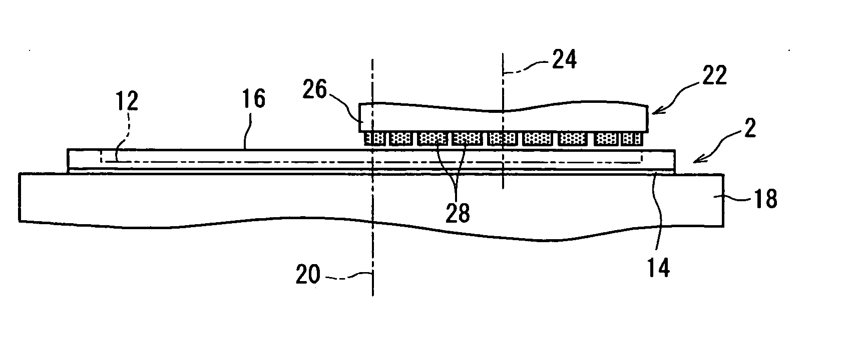
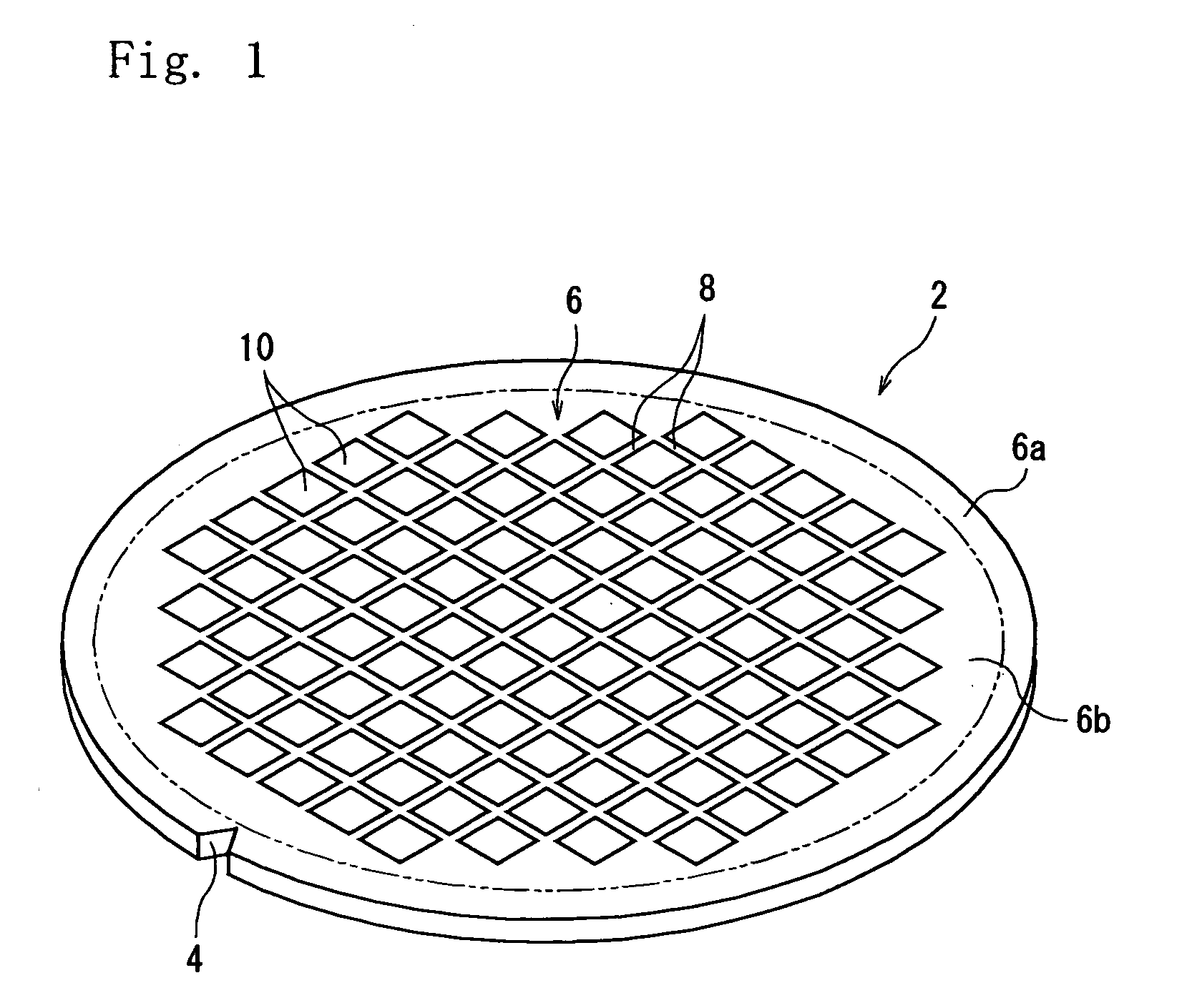
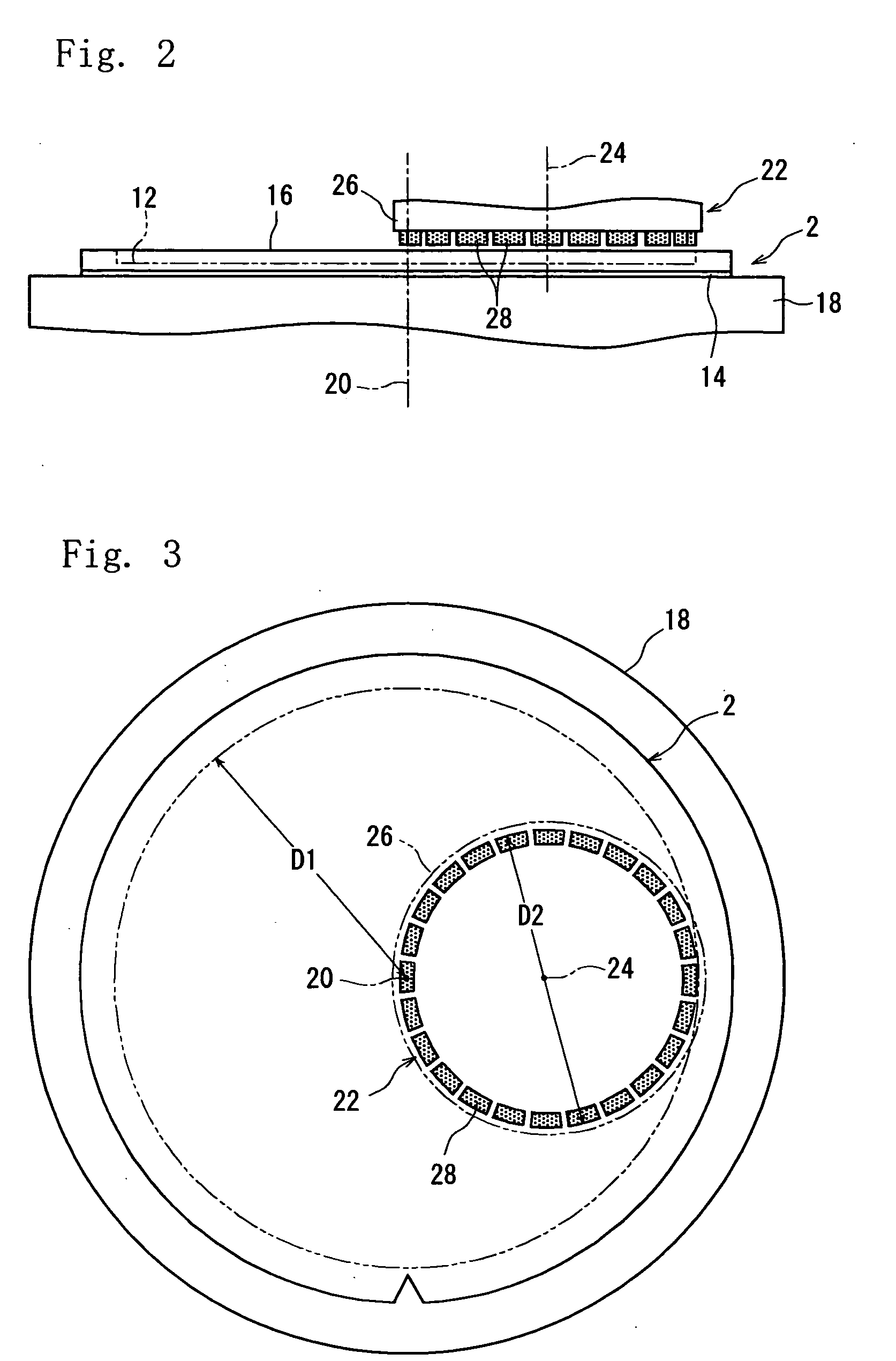
[0020]FIG. 1 shows a typical example of a semiconductor wafer 2 well known per se before being processed which is subjected to processing (to be described later) to configure a semiconductor wafer according to the present invention. The illustrated wafer 2 is circular as a whole, and has an orientation notch 4 formed in a circumferential edge portion thereof. The thickness of the wafer 2 is uniform throughout, and is preferably 250 μm or more, especially 300 to 700 μm. On the face 6 of the wafer 2 there are an annular surplus region 6a present in an outer peripheral edge portion of the face 6, and a circular device region 6b surrounded with the surplus region 6a. The notch 4 is formed in the annular surplus region 6a. The circular device region 6b has many rectangular regions 10 partitioned by streets 8 arranged in a lattice pattern, and a semiconductor device is disposed in each of the rectangular regions 10.

[0021] In the present invention, a circular concavity 12 (FIG. 4) is form...


PUM


Abstract

A semiconductor wafer which is generally circular, and which has on its face an annular surplus region present in an outer peripheral edge portion of the face, and a circular device region surrounded by the surplus region, the device region having many semiconductor devices disposed therein. A circular concavity is formed in the back of the semiconductor wafer in correspondence with the device region, and the device region is relatively thin, while the surplus region is relatively thick.

Description

FIELD OF THE INVENTION [0001] This invention relates to a semiconductor wafer which is generally circular, and which has on the face thereof a surplus region present in an outer peripheral edge portion of the face, and a circular device region surrounded by the surplus region, the device region having many semiconductor devices disposed therein; and a processing method for such a semiconductor wafer. DESCRIPTION OF THE PRIOR ART [0002] As is well known among people skilled in the art, it is common practice in the manufacture of a semiconductor device to dispose many semiconductor devices on the face of a generally circular semiconductor wafer, then grind the back of the semiconductor device to decrease the thickness of the semiconductor device to a required value, then, if necessary, conduct a required test, such as a probe test, on each of the semiconductor devices, and then dice the semiconductor wafer to separate the semiconductor devices individually. [0003] In recent times, it ...

Claims


Application Information

Patent Timeline
IPC IPC(8): H01L29/00
CPCH01L21/78H01L21/08H01L21/304H01L23/32
Inventor SEKIYA, KAZUMA
Owner DISCO CORP
Why Eureka
Try Eureka