Plasma display panel
a plasma display and panel technology, applied in the direction of instruments, manufacturing tools, electrodes, etc., can solve the problems of conventional pdp and other problems
- Summary
- Abstract
- Description
- Claims
- Application Information
AI Technical Summary
Benefits of technology
Problems solved by technology
Method used
Image
Examples
first embodiment example
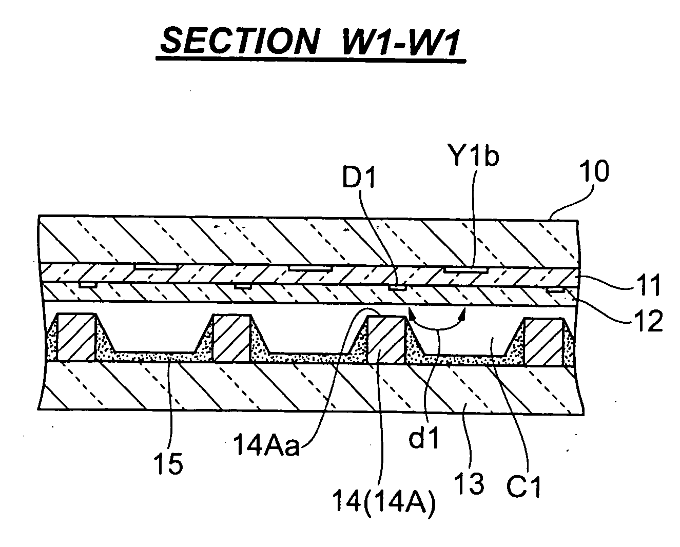
[0055]FIGS. 5 and 6 illustrate a first example of the embodiment of the PDP according to the present invention. FIG. 5 is a schematic front view showing the structure of a display line of the PDP in the first embodiment example, and FIG. 6 is a sectional view taken along the W1-W1 line in FIG. 5.
[0056] In FIGS. 5 and 6, row electrode pairs (X1, Y1) are formed on a front glass substrate 10 serving as the display surface and extend in the row direction of the front glass substrate 10 (the right-left direction in FIG. 5).
[0057] The row electrodes X1 and Y1 are each composed of belt-shaped bus electrodes X1a, Y1a extending parallel to each other in the row direction and formed of a black- or dark-colored metal film, and a plurality of transparent electrodes X1b, Y1b which are spaced at regular intervals and connected to the associated bus electrodes X1a, Y1a, and each extend out from the associated bus electrodes X1a, Y1a toward their counterparts in the row electrode pair so as to fa...
second embodiment example
[0071]FIGS. 7 and 8 illustrate a second example of the embodiment of the PDP according to the present invention. FIG. 7 is a schematic front view showing the structure of a display line of the PDP in the second embodiment example, and FIG. 8 is a sectional view taken along the W2-W2 line in FIG. 7.
[0072] In FIGS. 7 and 8, column electrodes D2 are formed on the rear-facing face of the first dielectric layer 11. Each of the column electrodes D2 extends in the column direction and parallel to the centerline between the adjacent transparent electrodes X1b and adjacent transparent electrodes Y1b which are spaced at regular intervals in the row direction along the associated bus electrodes X1a, Y1a of the row electrodes X1, Y1.
[0073] The structure of the other components provided on the front glass substrate 10 in the second embodiment example is approximately the same as that in the PDP of the first embodiment example, and the same components are designated by the same reference numera...
third embodiment example
[0084]FIGS. 9 and 10 illustrate a third example in the embodiment of the PDP according to the present invention. FIG. 9 is a schematic front view showing the structure of a display line of the PDP in the third embodiment example, and FIG. 10 is a sectional view taken along the W3-W3 line in FIG. 9.
[0085] In FIGS. 9 and 10, the column electrodes D2 are formed on the rear-facing face of the first dielectric layer 11. Each of the column electrodes D2 extends in the column direction and parallel to the centerline between the adjacent transparent electrodes X1b and adjacent transparent electrodes Y1b which are regularly spaced in the row direction along the associated bus electrodes X1a, Y1a of the row electrodes X1, Y1.
[0086] The above structure is approximately the same as that in the PDP of the second embodiment example and the same components are designated by the same reference numerals.
[0087] Additional dielectric layers 22 project from the rear-facing face of the first dielectr...
PUM
| Property | Measurement | Unit |
|---|---|---|
| area | aaaaa | aaaaa |
| thickness | aaaaa | aaaaa |
| distance | aaaaa | aaaaa |
Abstract
Description
Claims
Application Information


