E-fuse circuit using leakage current path of transistor

a leakage current path and transistor technology, applied in the field of fuse circuits, can solve the problems of not providing the ability to repair a memory device, adversely affecting the manufacturing yield of the memory device, and often considered inutility of the entire memory device, so as to improve the reproducibility and reliability of programming, improve the effect of immunity and high programming voltag

Inactive Publication Date: 2006-11-02
SAMSUNG ELECTRONICS CO LTD
View PDF9 Cites 5 Cited by
  • Summary
  • Abstract
  • Description
  • Claims
  • Application Information

AI Technical Summary

Benefits of technology

[0012] Embodiments of the invention provide an e-fuse exhibiting improved reproducibility and reliability of programming despite potential variations in process. Embodiments of the invention also enjoy much greater immunity to relatively high programming voltage and relatively excessive programming current.

Problems solved by technology

Should only a few of these memory cells be defective, the entire memory device is often considered unusable.
Thus, the consistent appearance of only a few bad memory cells in a much larger array of memory cells will adversely affect manufacturing yield for the memory device.
However, such programming techniques do not provide an ability to repair a memory device once it is placed into a package.
This type of limitation resulted in the development of an electronic fuse (“e-fuse”).
Unfortunately, consistent (i.e., highly reliable and reproducible) programming results are sometime difficult to obtain, since a fuse's response to an applied program current may vary in accordance with certain fabrication process variations.
Thus, if a relatively excess program current is applied, heat may be generated in and around the fuse before the fuse is properly programmed.
This heat may damage certain layers of the semiconductor device and / or result in low reproducibility and reliability of the fuse programming operation.

Method used


Image

  • E-fuse circuit using leakage current path of transistor
  • E-fuse circuit using leakage current path of transistor
  • E-fuse circuit using leakage current path of transistor

Examples


Embodiment Construction

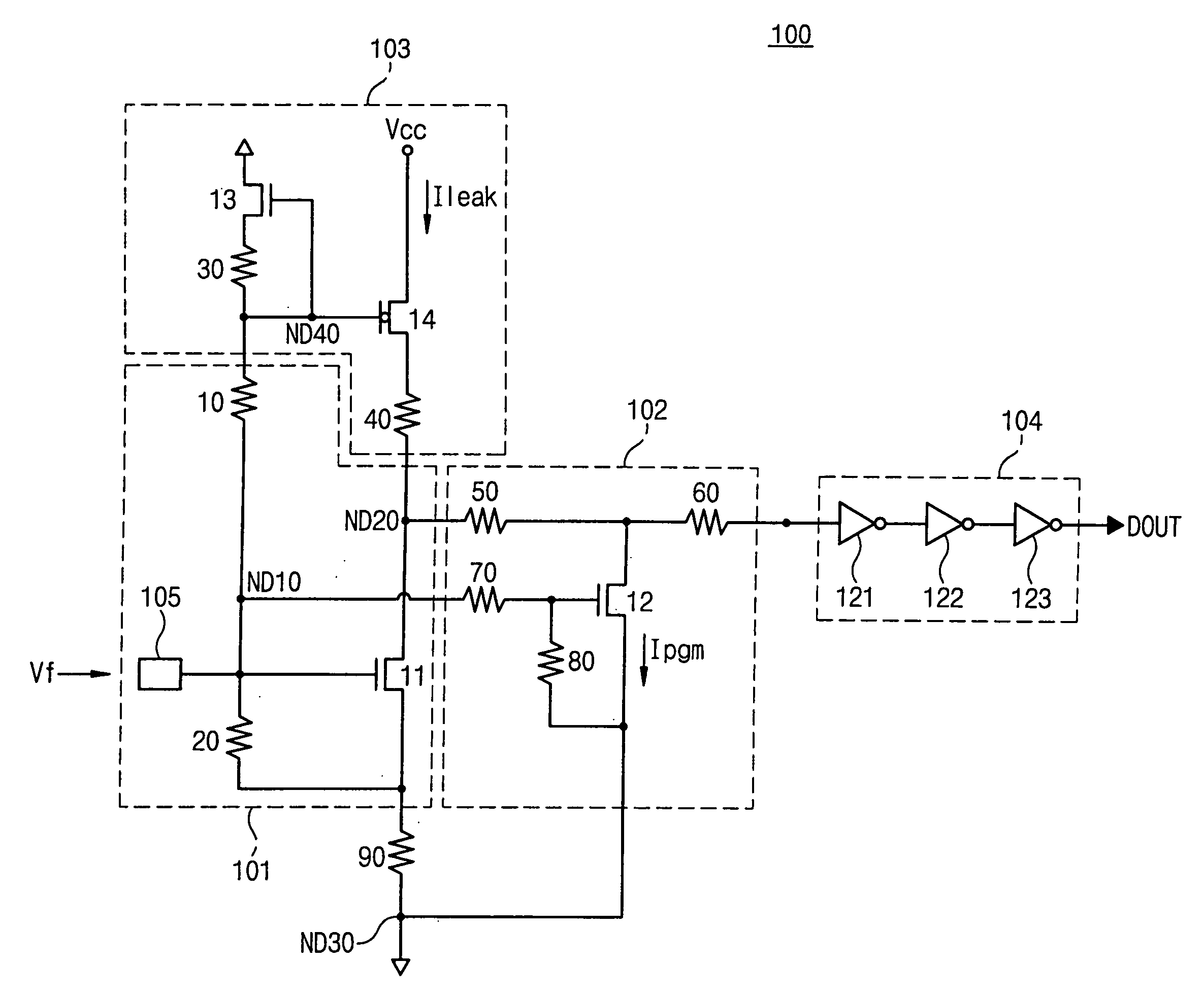
[0016] Reference will now be made to certain embodiments of the invention. However, it should be noted that the invention is not limited to only the illustrated embodiments. Rather, the embodiments are presented as teaching examples. The scope of the invention is defined by the claims that follow.

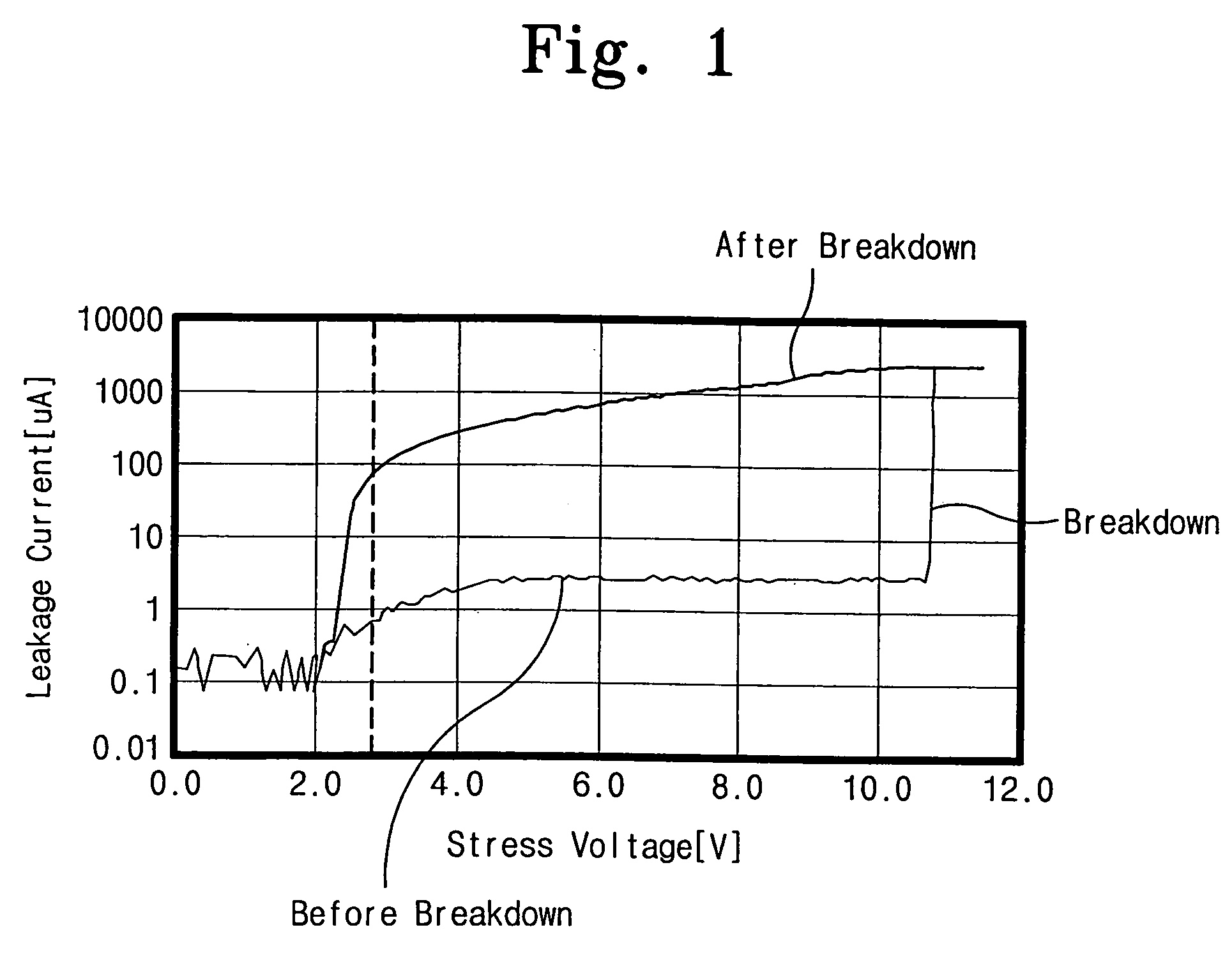
[0017]FIG. 1 is a graph showing dielectric breakdown strength characteristic of a generic semiconductor transistor. The horizontal axis of the graph denotes a stress voltage applied to the gate of the transistor. The vertical axis of graph denotes a corresponding leakage current flowing between the gate and drain or between the gate and source.

[0018] With reference to FIG. 1, a dielectric breakdown occurs in the generic transistor when a stress voltage of about 11V is applied. Prior to dielectric breakdown, the leakage current for the transistor flowing between the gate and drain, or between the gate and source is fairly steady at one to several micro-amperes. However, after dielectric br...


PUM


Abstract

An e-fuse adapted to indicate programming state in relation leakage current path defined by a program transistor both before and after dielectric breakdown has occurred. The e-fuse comprises: a program circuit including the program transistor, a switch circuit connected between the program circuit and ground, a current supply circuit connected to the program circuit and supplying a predetermined current to the leakage current path after the program transistor is programmed; and a sense/amplification circuit connected to a program node associated with the leakage current path and adapted to sense and output the programming state.

Description

BACKGROUND OF THE INVENTION [0001] 1. Field of the Invention [0002] Embodiments of the invention relate to a fuse circuit. More particularly, embodiments of the invention relate to an e-fuse circuit using a transistor leakage current path. [0003] 2. Description of the Related Art [0004] Fuse circuits are regularly included with semiconductor circuits for a number of different reasons. For example, many semiconductor memory circuits include a collection of fuses as part of circuitry enabling memory redundancy. In this context, it is well known that memory devices, such as Dynamic Random Access Memory (DRAM), are manufactured to include a large number of memory cells. Should only a few of these memory cells be defective, the entire memory device is often considered unusable. Thus, the consistent appearance of only a few bad memory cells in a much larger array of memory cells will adversely affect manufacturing yield for the memory device. As a result, provision for a number of redunda...

Claims


Application Information

Patent Timeline
Patent Type & Authority Applications(United States)
IPC IPC(8): H01H37/76
CPCH01L23/5252G11C17/18H01L2924/0002H01L2924/00G11C5/14G11C7/06G11C17/16G11C29/787
Inventor CHOI, JEONG-UNHWANG, SO-HEE
Owner SAMSUNG ELECTRONICS CO LTD
Why Eureka
Try Eureka