Liquid crystal display and manufacturing method of the same

Inactive Publication Date: 2006-11-02
SAMSUNG ELECTRONICS CO LTD
View PDF10 Cites 10 Cited by
  • Summary
  • Abstract
  • Description
  • Claims
  • Application Information

AI Technical Summary

Benefits of technology

[0011] Accordingly, it is an aspect of the present invention to provide a liquid crystal display (“LCD”) and a manufacturing method of the same realizing a wide angular field and improving a response time of a liquid crystal.

Problems solved by technology

However, an aforementioned method of providing the cutting pattern and the projection has a disadvantage, that is, an additional process is needed to form the cutting pattern or the projection on the pixel electrode and on the common electrode, respectively.
Moreover, since the liquid crystal molecules adjacent to the cutting pattern or the projection are strongly influenced by the fringe field, they are quickly realigned, but the liquid crystal molecules far from the cutting pattern or the projection are instead influenced by the liquid crystal molecules adjacent to the cutting pattern or the projection and are then realigned, therefore the response time of the liquid crystal molecules far from the cutting pattern or the projection is disadvantageously slow.
In addition, in case of a weak fringe field by the cutting pattern, the liquid crystal molecules are not properly oriented and the response time of the liquid crystal is disadvantageously slow.

Method used


Image

  • Liquid crystal display and manufacturing method of the same
  • Liquid crystal display and manufacturing method of the same
  • Liquid crystal display and manufacturing method of the same

Examples


first embodiment

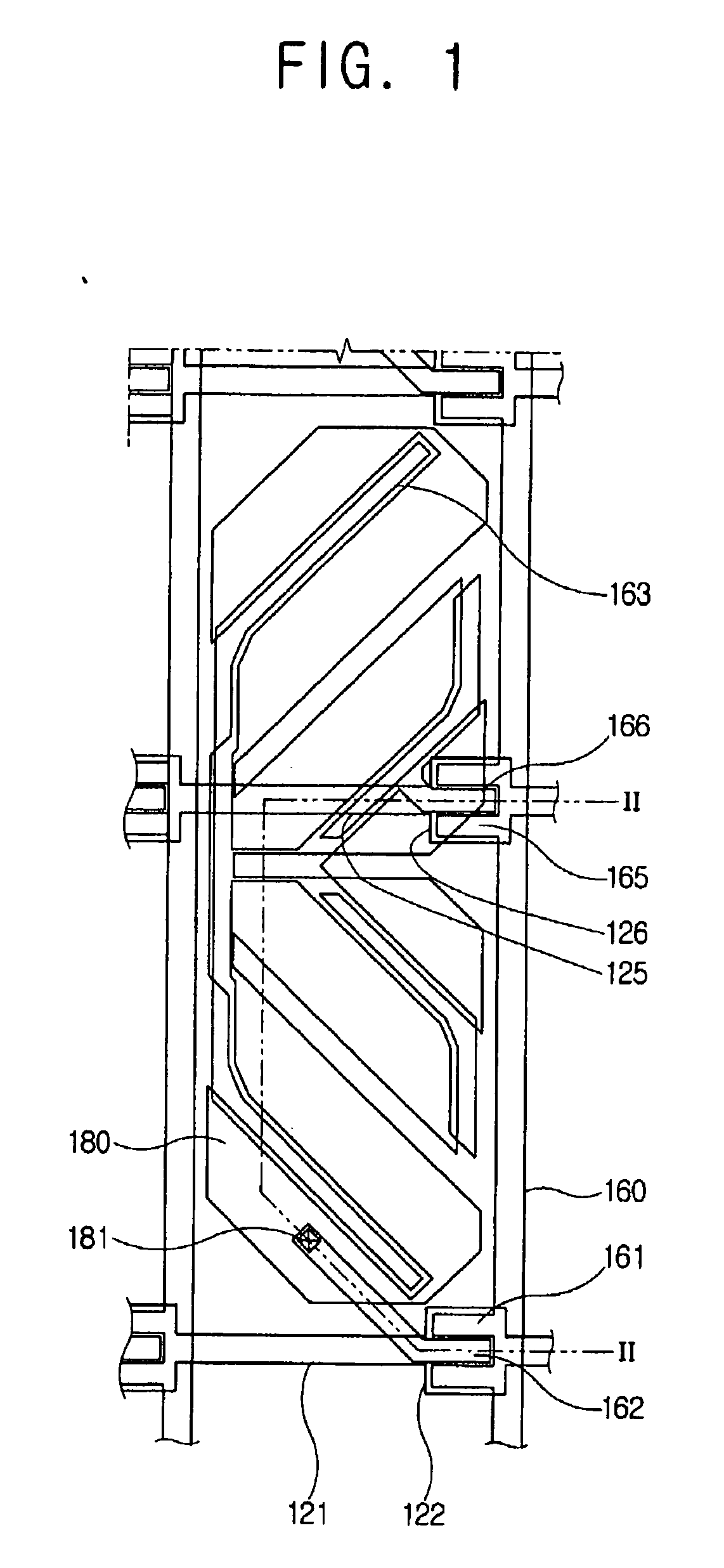
[0092] Hereinafter, an exemplary driving method according to the present invention will be described with reference to FIGS. 6A and 6B. FIG. 6A shows how a data signal and a gate signal are applied when a single gate is driven and FIG. 6B shows how a data signal and a gate signal are applied when a dual gate is driven.

[0093] As shown in FIG. 6A, in an upper graph showing a signal applied to a data line 160, a first γ-voltage is a picture signal applied to a pixel electrode 180 and a second γ-voltage is a direction control signal applied to a direction control electrode line 163. A middle graph shows the gate signal applied to a TFT(T2) for a direction control electrode and a lower graph shows a gate signal applied to a TFT(T1) for a pixel electrode 180. As shown in the graphs, the direction control signal applied to the direction control electrode line 163 rises and falls before the picture signal applied to the pixel electrode 180 does at a predetermined time, voltage applied to th...

third embodiment

[0117] Here, a projection 265 shown in the third embodiment, as illustrated in FIG. 8, may be formed by using an exposure degree and a developing process.

[0118] Thereafter, adhering the first and the second substrates 100, 200, interposing the liquid crystal layer 300 between the two substrates 100, 200, and going through the module process, thereby completes the LCD.

second embodiment

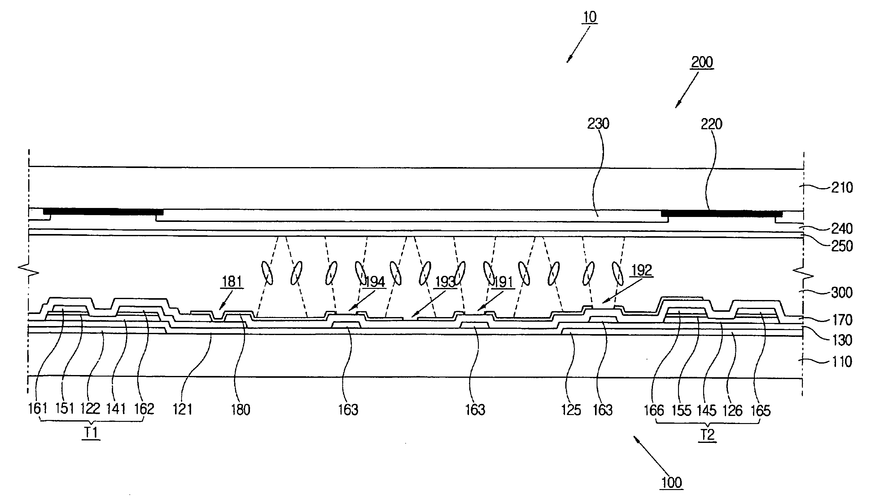
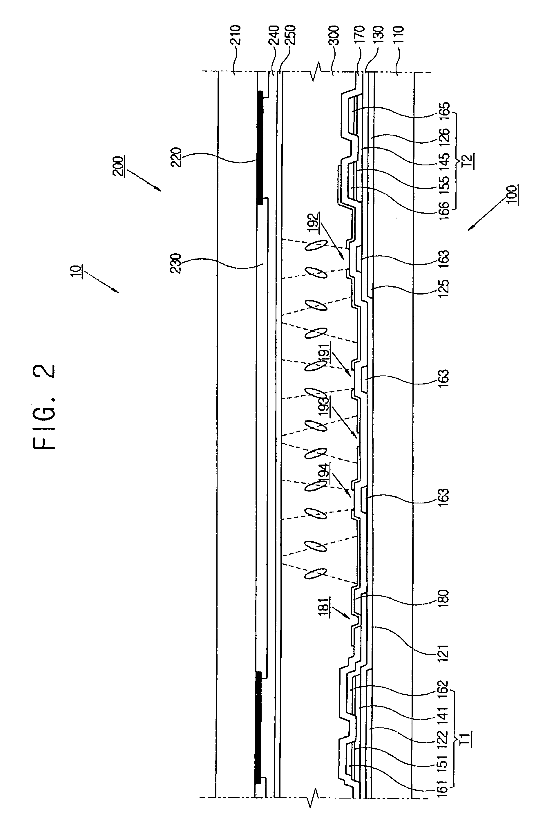
[0119] When the fringe field is weakly flown out by the direction control electrode line 163 and a plurality of domains where liquid crystal molecules tilt in different directions are not formed, the organic layer mountain structure-type pattern 260 described in the second embodiment, illustrated in FIG. 7, makes the fringe field strong, thereby a pixel is divided into a plurality of domains by a pixel electrode cutting pattern 190 and the direction control electrode line 163 and the liquid crystal molecules are differently aligned in each domain, therefore, a wide angular field may be realized.

[0120] When the liquid crystal molecules are given the pretilt by the organic layer mountain structure-type pattern 260 and predetermined voltage is applied to the pixel electrode 180, the liquid crystal molecules are quickly realigned, thereby improving a response time.

[0121] Also, if a fringe field is weak even when employing the organic layer mountain structure-type pattern 260, if the pr...


PUM


Abstract

An LCD includes first and second insulating substrates with liquid crystal disposed therebetween, first and second gate lines, a data line crossed and insulated with the gate lines, thereby defining a pixel area, a pixel electrode formed in the pixel area and having a pixel electrode cutting pattern, a direction control electrode line electrically separated from the pixel electrode, at least partly overlapped with the pixel electrode cutting pattern and controlling the liquid crystal layer, a TFT for the pixel electrode formed in an area where the first gate line and the data line are crossed and connected to the pixel electrode, and a TFT for a direction control electrode formed in an area where the second gate line and the data line are crossed and connected to the direction control electrode line. Accordingly, an LCD realizes a wide angular field and improves a response time of a liquid crystal.

Description

[0001] This application claims priority to Korean Patent Application No. 2005-0036796, filed on May 2, 2005 and all the benefits accruing therefrom under 35 U.S.C. §119, and the contents of which in its entirety are herein incorporated by reference. BACKGROUND OF THE INVENTION [0002] 1. Field of the Invention [0003] The present invention relates to a liquid crystal display (“LCD”) and a manufacturing method of the same. More particularly, the present invention relates to an LCD and a manufacturing method of the same dividing a single pixel into a plurality of domains, thereby realizing a wide angular field and improving response time of a liquid crystal. [0004] 2. Description of the Related Art [0005] A liquid crystal display (“LCD”) is widely used as a flat panel display since it is not only slim and light, but it also consumes less electric power than a cathode-ray tube (“CRT”). [0006] The LCD includes an LCD panel having a thin film transistor (“TFT”) substrate on which TFTs are ...

Claims


Application Information

Patent Timeline
IPC IPC(8): G02F1/1343
CPCG02F1/13624G02F1/133707G02F1/1343
Inventor SOHN, JI-WONCHOI, NAK-CHO
Owner SAMSUNG ELECTRONICS CO LTD
Why Eureka
Try Eureka