Semiconductor light emitting device

a technology of semiconductors and light emitting devices, which is applied in the direction of solid-state devices, lighting and heating devices, lighting support devices, etc., can solve the problems of poor color rendering properties, difficult to produce leds with high brightness and excellent color rendering properties, and inability to provide bright red colors. , to achieve the effect of excellent color rendering properties and high brightness

Active Publication Date: 2006-11-02
XIAMEN SANAN OPTOELECTRONICS CO LTD
View PDF9 Cites 107 Cited by
  • Summary
  • Abstract
  • Description
  • Claims
  • Application Information

AI Technical Summary

Benefits of technology

[0013] One object of the present invention is to provide a semiconductor light emitting device having high brightness and excellent color rendering properties.
[0015] According to the present invention, a semiconductor light emitting device having high brightness and excellent color rendering properties can be provided.

Problems solved by technology

Since each of these conventional devices has advantages and disadvantages as described below, it has been difficult to produce an LED having high brightness and excellent color rendering properties.
As a result, the device having LEDs of white light emitting type has poor color rendering properties, and in particular it cannot provide bright red color.
Although some fluorescent substances allow the device of this type to have a red component, using such a fluorescent substance to achieve the above effect involves poor efficiency.
Furthermore, since the device having LEDs of white light emitting type cannot display individual colors such as blue, green, and the like, its application is limited.
However, when compared with the device having LEDs of white light emitting type each formed by exciting a blue LED with a fluorescent substance, it is difficult for the device of this type to achieve brightness due to a problem in individual light emission efficiency.

Method used


Image

  • Semiconductor light emitting device
  • Semiconductor light emitting device
  • Semiconductor light emitting device

Examples


Embodiment Construction

[0029] Referring to the drawings, embodiments of the present invention will be described.

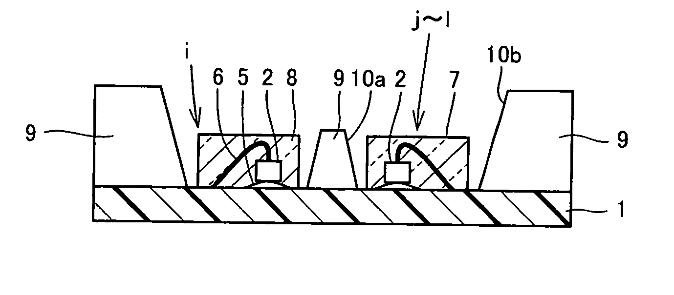
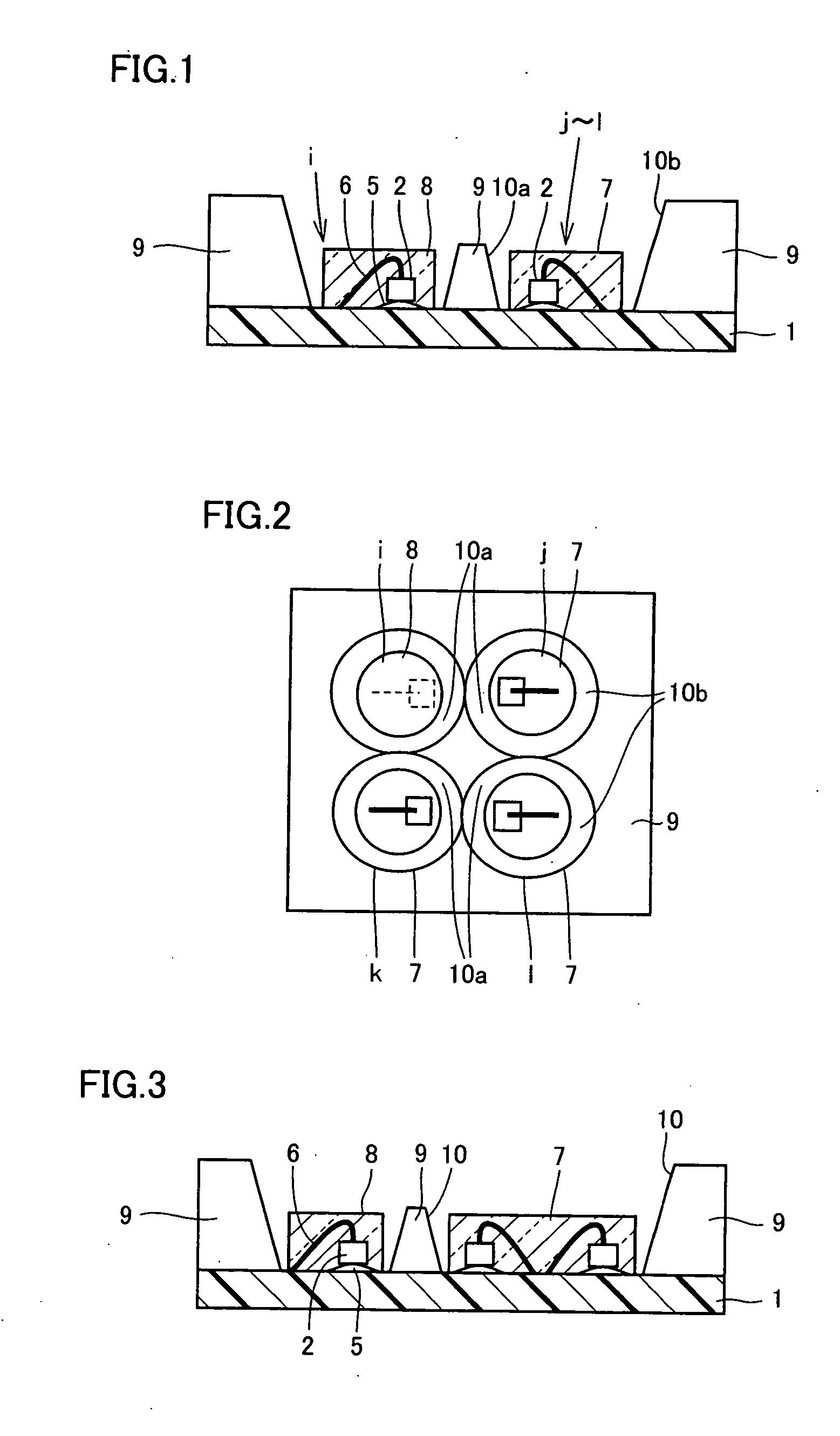
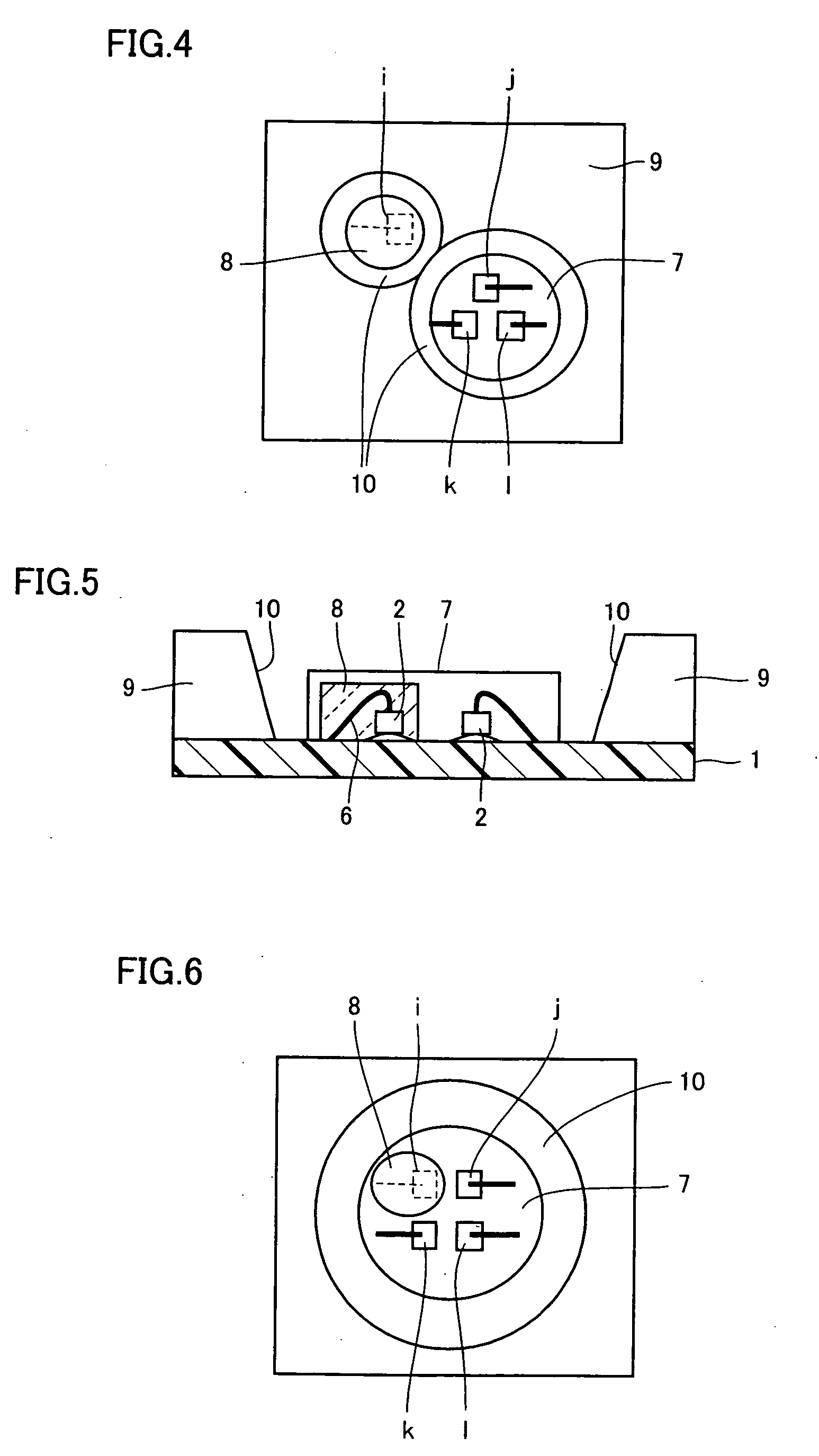
[0030]FIGS. 1 and 2 are a cross sectional view and a plan view, respectively, of a surface mounted LED showing an embodiment of a semiconductor light emitting device of the present invention.

[0031] The semiconductor light emitting device has a substrate 1 with a terminal (not shown) formed thereon for electrically connecting substrate 1 with an external interconnection. On substrate 1 are provided elements 2 emitting light in four different colors. The four different colors include red, green, blue, and white. Element 2 is formed of a light emitting diode element (hereinafter, element 2 will also be referred to as an “LED chip”).

[0032] On the surface of substrate 1 is formed pattern interconnection electrically connecting an electrode of each element 2 with the terminal (not shown), and LED chip 2 is mounted thereon. Specifically, LED chip 2 is electrically and mechanically connected with sub...


PUM


Abstract

A semiconductor light emitting device of the present invention includes four elements provided on a substrate and having different light emitting colors of red, green, blue, and white, respectively; a resin covering each of the elements; and a reflector provided to surround a circumference of the resin. With this structure, a semiconductor light emitting device having high brightness and excellent color rendering properties can be provided.

Description

[0001] This nonprovisional application is based on Japanese Patent Application No. 2005-132334 filed with the Japan Patent Office on Apr. 28, 2005, the entire contents of which are hereby incorporated by reference. BACKGROUND OF THE INVENTION [0002] 1. Field of the Invention [0003] The present invention relates to a semiconductor light emitting device using a light emitting element such as a light emitting diode (LED). [0004] 2. Description of the Background Art [0005] A semiconductor light emitting device of this kind is disclosed for example in Japanese Patent Laying-Open No. 2000-269551. [0006] This conventional device typically has a structure of a surface mounted LED as shown in FIG. 12. In this conventional structure, a resin b to fix a lead frame a is formed by insert molding or the like. On lead frame a, an LED chip c is electrically and mechanically connected by means of an Ag paste f and a gold wire d. The circumference of LED chip c is protected and sealed with an epoxy r...

Claims


Application Information

Patent Timeline
Patent Type & Authority Applications(United States)
IPC IPC(8): F21V9/00H01L33/50H01L33/56H01L33/60H01L33/62
CPCH01L25/0753H01L33/483H01L33/60H01L2224/73265H01L2924/01322H01L2224/48091H01L2224/45144H01L2924/3025H01L2924/00014H01L2924/00H01L33/486
Inventor TAKENAKA, YASUJI
Owner XIAMEN SANAN OPTOELECTRONICS CO LTD
Why Eureka
Try Eureka