

Semiconductor film manufacturing method and substrate manufacturing method
- Summary
- Abstract
- Description
- Claims
- Application Information
AI Technical Summary
Benefits of technology
Problems solved by technology
Method used
Image

Examples
first embodiment
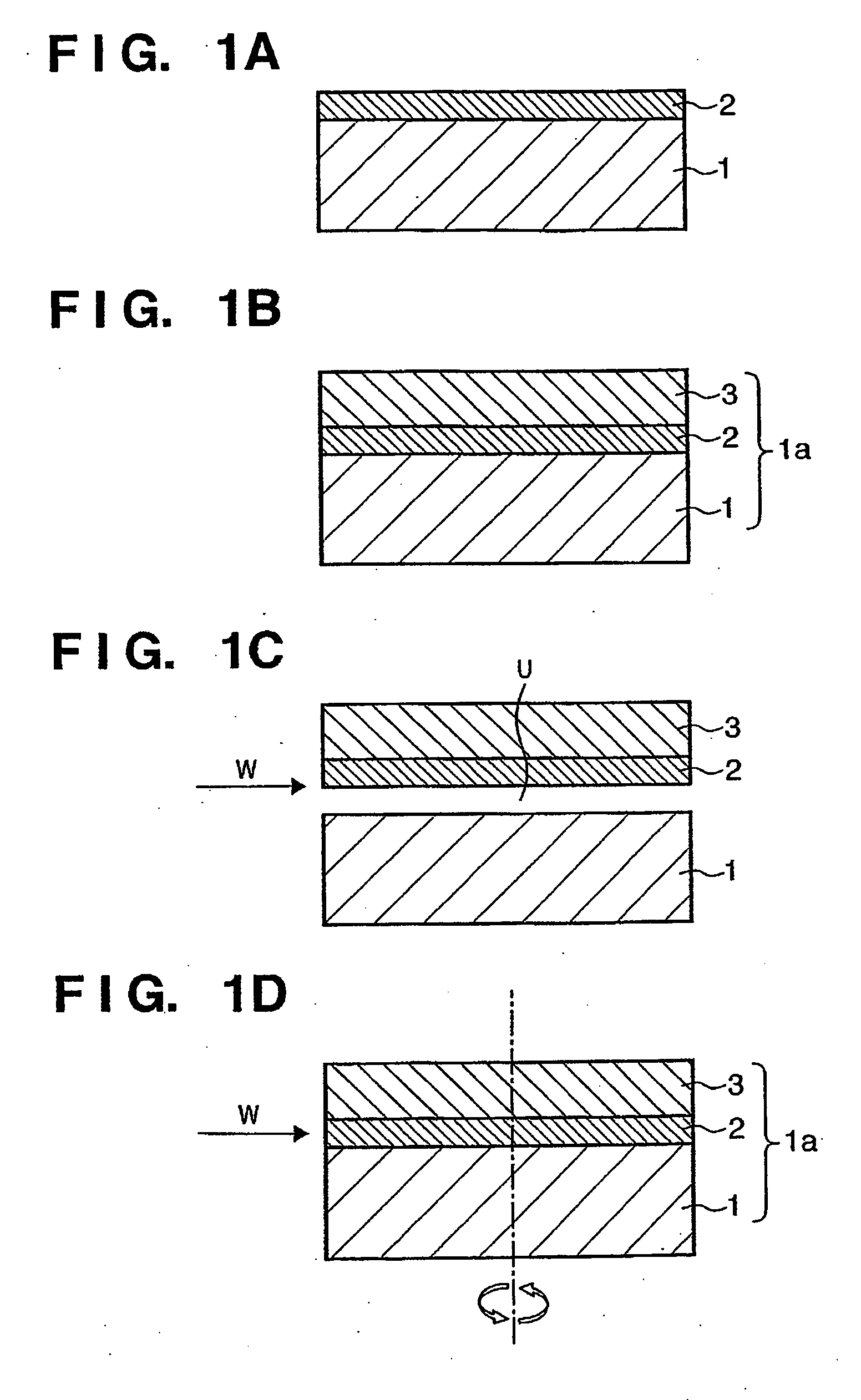
[0047] As the first embodiment of the present invention, a method of separating a semiconductor film from a substrate or a method of manufacturing a semiconductor film separated from a substrate will be described below. FIGS. 1A to 1D are views schematically showing a method of separating a semiconductor film from a substrate or method of manufacturing a semiconductor film separated from a substrate.
[0048] In the separation layer forming step shown in FIG. 1A, on a seed substrate 1 such as a Ge substrate having crystallinity, a semiconductor film having a lattice constant different from the seed substrate 1, and for example, a separation layer 2 made of AlAs or InGaAs is hetero-epitaxially grown.
[0049] In the semiconductor film forming step shown in FIG. 1B, a semiconductor film 3 made of GaAs is formed on the separation layer 2 to form a composite member 1a including the substrate 1, separation layer 2, and semiconductor film 3. At this time, a semiconductor de...
second embodiment
Substrate Manufacturing Method
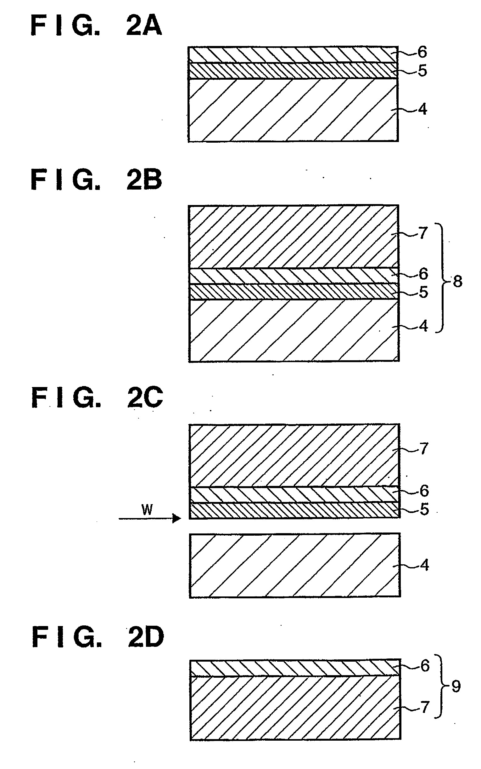
[0064] As the second embodiment of the present invention, a method of manufacturing a substrate having a semiconductor film will be described below. FIGS. 2A to 2D are views schematically showing a method of manufacturing a substrate having a semiconductor film.
[0065] In the step shown in FIG. 2A (separation layer forming step and semiconductor film forming step), on a first substrate (seed substrate) 4 such as a Ge substrate having crystallinity, a semiconductor film having a lattice constant different from the first substrate 4, and for example, a separation layer 5 made of InGaAs is hetero-epitaxially grown. A semiconductor film 6 made of GaAs is formed on the separation layer 5.
[0066] In the bonding step shown in FIG. 2B, the first substrate 4 is bonded to a second substrate (handle substrate) 7 such as an Si substrate while setting the semiconductor film 6 inside to form a composite member composite substrate) 8. In this bonding, when a metal fi...
third embodiment
Semiconductor Device Manufacturing Method
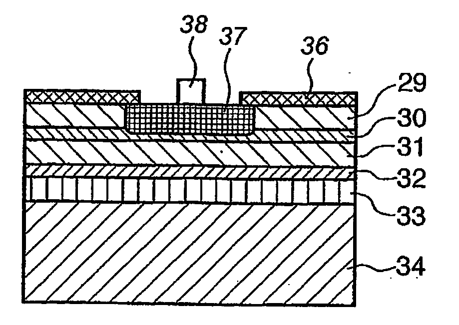
[0074] As the third embodiment of the present invention, a method of manufacturing a semiconductor film having a semiconductor device or a substrate will be described below. FIGS. 3A to 3E are views schematically showing a method of manufacturing a semiconductor film having a semiconductor device or a substrate.
[0075] In the step shown in FIG. 3A (separation layer forming step and semiconductor film forming step), on a first substrate (seed substrate) 10 such as a Ge substrate having crystallinity, a semiconductor film having a lattice constant different from the first substrate 10, and for example, a separation layer 11 made of InGaAs is hetero-epitaxially grown. A semiconductor film 12 made of GaAs is formed on the separation layer 11.
[0076] In the semiconductor device forming step shown in FIG. 3B, a semiconductor device 13 such as an LED is formed in the semiconductor film 12. Typically, in the semiconductor device forming step, instea...
PUM
 Abstract
Description
Claims
Application Information