Miniaturized multi-chip module and method for manufacturing the same

Active Publication Date: 2006-11-09
UNIVERSAL SCIENTIFIC INDUSTRIAL (SHANGHAI) CO LTD
View PDF5 Cites 7 Cited by
  • Summary
  • Abstract
  • Description
  • Claims
  • Application Information

AI Technical Summary

Benefits of technology

[0018] 3. The ball-planting machine for planting the solder balls 23 is an expensive piece of equipment. Purchasing the ball-planting machine results in higher capital costs for

Problems solved by technology

The ball-planting machine for planting the solder balls 23 is an expensive piece of equipment.
Purchasing the ba

Method used


Image

  • Miniaturized multi-chip module and method for manufacturing the same
  • Miniaturized multi-chip module and method for manufacturing the same
  • Miniaturized multi-chip module and method for manufacturing the same

Examples


Embodiment Construction

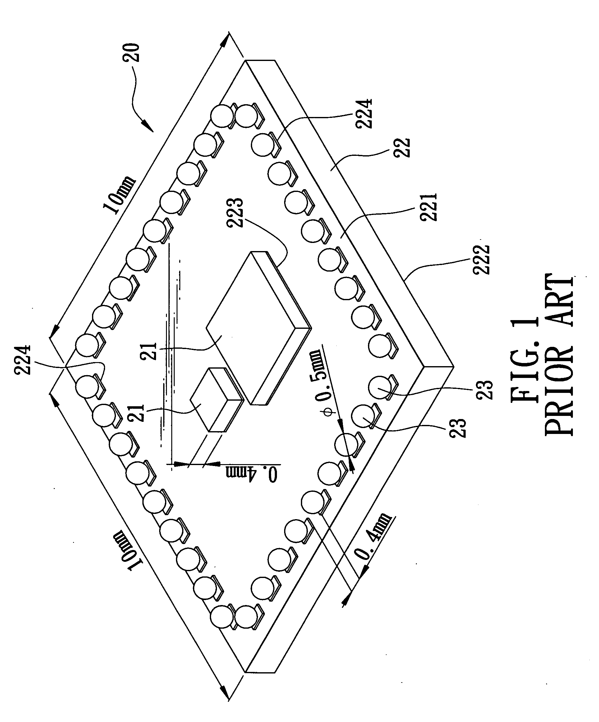
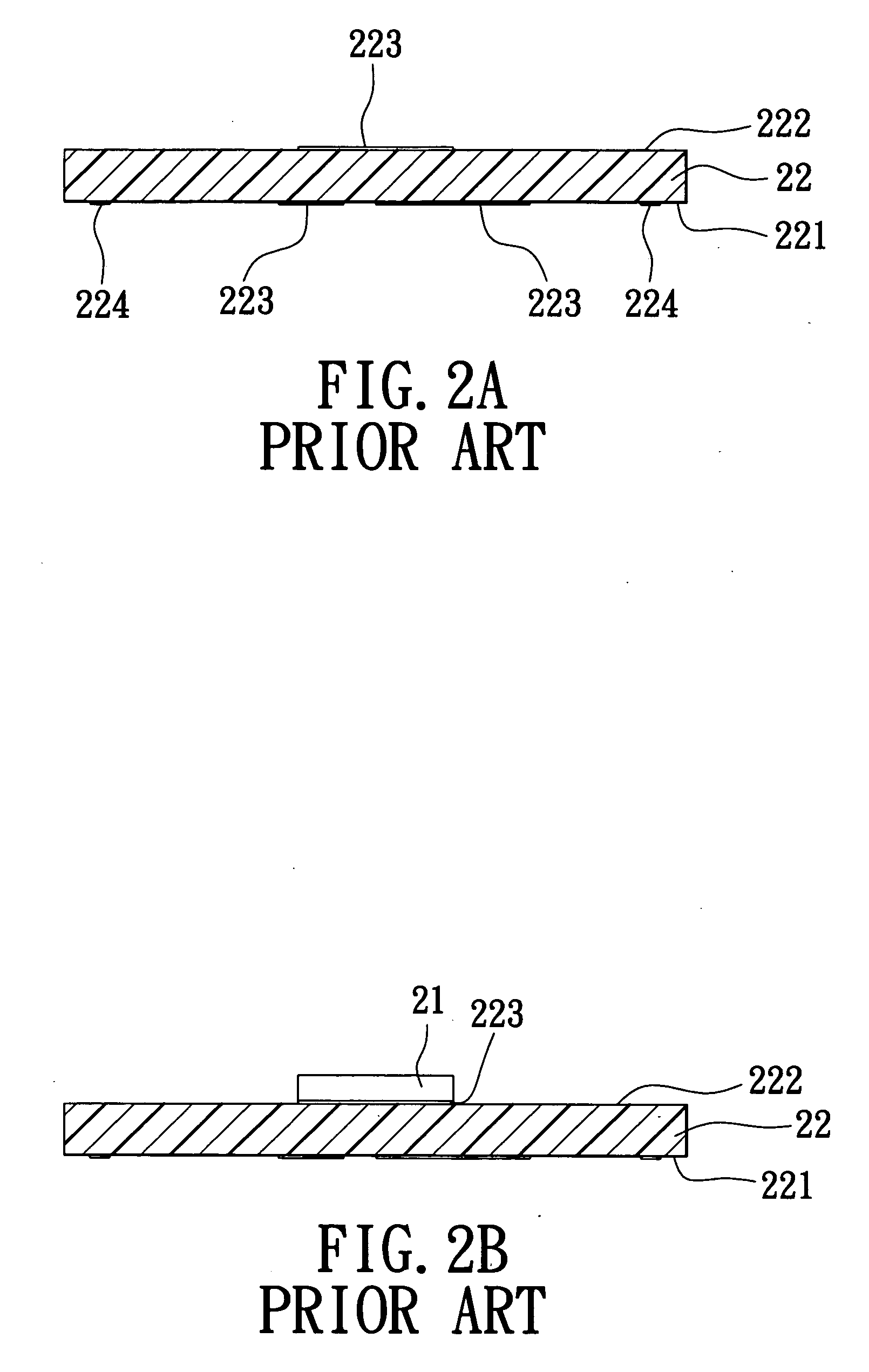
[0043] Before the present invention is described in greater detail, it should be noted that like elements are denoted by the same reference numerals throughout the disclosure.

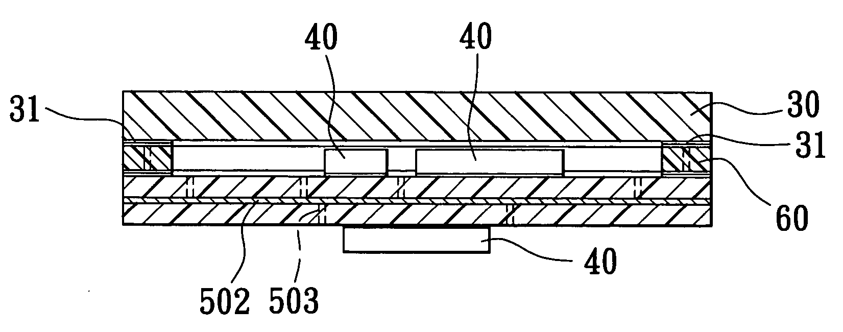
[0044] Referring to FIGS. 3 and 4, the first preferred embodiment of a miniaturized multi-chip module 400 according to the present invention is adapted for mounting on a circuit board 30 (see FIG. 6F) of a target device so as to establish electrical connection therewith. In this embodiment, the miniaturized multi-chip module 400 provides the target device with a wireless transmission capability when mounted on the circuit board 30, and includes a substrate 50, a plurality of integrated circuit chips 40 (there are three integrated circuit chips 40 in this embodiment, as best shown in FIGS. 6E and 6F), and an interposer 60.

[0045] One of the integrated circuit chips 40 is a commercially available chip having a wireless transmission capability, such as a WLAN chip, Bluetooth chip, WiMAX chip, UWB chip, DTV receiv...


PUM


Abstract

A miniaturized multi-chip module suitable for application to wireless transmission devices includes a substrate, integrated circuit chips mounted on and connected electrically to the substrate, and an interposer mounted on one surface of the substrate. The interposer cooperates with the substrate to confine a receiving space for receiving the integrated circuit chips on the surface of the substrate to which the interposer is attached, and is provided with conductors that are connected electrically to the substrate. Therefore, when the interposer is mounted on a circuit board, the conductors serve as external electrical connections for the integrated circuit chips. A method for manufacturing the miniaturized multi-chip module is also disclosed.

Description

CROSS-REFERENCE TO RELATED APPLICATION [0001] This application claims priority of Taiwanese application no. 094114516, filed on May 5, 2005. BACKGROUND OF THE INVENTION [0002] 1. Field of the Invention [0003] The invention relates to a multi-chip module, more particularly to a miniaturized multi-chip module suitable for application to wireless transmission devices and to a method for manufacturing the same. [0004] 2. Description of the Related Art [0005]FIG. 1 illustrates a conventional multi-chip module 20 for application to a wireless transmission device (not shown). The multi-chip module 20 includes a plurality of integrated circuit chips 21, a module substrate 22, and a plurality of solder balls 23. [0006] One of the integrated circuit chips 21 has a wireless transmission capability. [0007] The module substrate 22 has a first surface 221, a second surface 222 opposite to the first surface 221, a plurality of first solder pads 223 formed on the first and second surfaces 221, 222,...

Claims


Application Information

Patent Timeline
IPC IPC(8): H01L23/34
CPCH01L23/49822H01L23/49838H01L23/5385H01L25/0657H05K1/141H01L2224/32225H05K3/3442H05K2201/2018H05K2203/1572H01L2225/0652H01L2225/06572H05K1/145
Inventor LIAO, KUO-HSIENCHEN, JIA-YANGWANG, CHUEI-TANG
Owner UNIVERSAL SCIENTIFIC INDUSTRIAL (SHANGHAI) CO LTD
Why Eureka
Try Eureka