Modular integrated circuit chip carrier

a module and integrated circuit technology, applied in the direction of electrical apparatus construction details, inspection/indentification of circuits, and association of printed circuits, can solve the problems of the very nature of bga connected devices, and the inability to directly or indirectly test bga connected devices

Inactive Publication Date: 2006-11-16
LEGACY ELECTRONICS INC
View PDF99 Cites 12 Cited by
  • Summary
  • Abstract
  • Description
  • Claims
  • Application Information

AI Technical Summary

Benefits of technology

[0010] It is an objective of the present invention to provide a method and apparatus that will allow for the stacking of semiconductor chips on a circuit board. It is a further objective of the present invention to provide a method and apparatus that can be integrated into current circuit board assembly operations without modification of existing practices. It is further objective of the present invention to provide a method and apparatus that can be used to stack semiconductor chips without the modification of existing semiconductor chip packages.
[0013] In another variation of the invention it provides a way to position the pads on which a chip rests directly over a descending via. It does this by filling in the hollow portions left in a via after its fabrication with a non-conductive or conductive filler material. This reduces the space necessary for the pads by avoiding the need to offset the pads from the vias.

Problems solved by technology

However, BGA types of connectors have their own problems among them being an inability to test the BGA connected device while it is connected into the circuitry of a board or other device.
On the other hand BGA connected devices by the very nature of the connection are impossible to directly or even indirectly test while they are connected into the circuit.
Another problem with BGA type of connectors is the need to develop new techniques that will allow for stacking chips since many if not most of the techniques used to stack chips are for integrated circuit packages that use leads and cannot be readily adapt to BGA type of connectors.
Additionally, most of the existing chip stacking devices and methods used to form chips into a three dimensional array tend to be very complicated.
They typically cannot work with standard IC packages, be they the lead type or BGA type and generally require the modification of the chip package itself for implementation.

Method used


Image

  • Modular integrated circuit chip carrier
  • Modular integrated circuit chip carrier
  • Modular integrated circuit chip carrier

Examples


Embodiment Construction

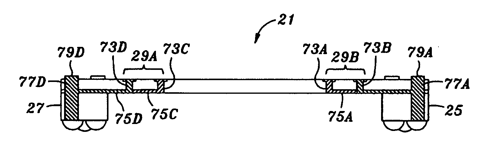
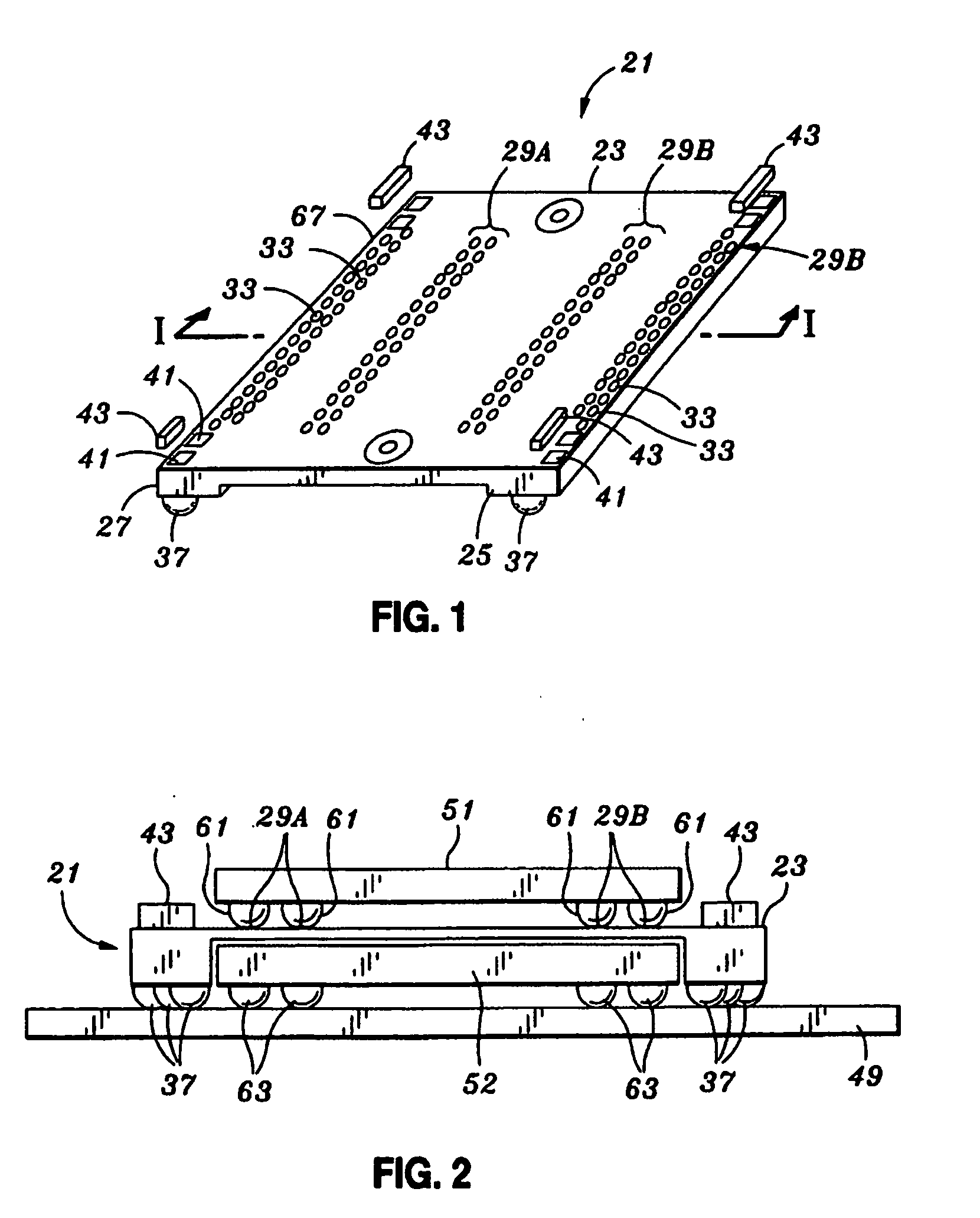
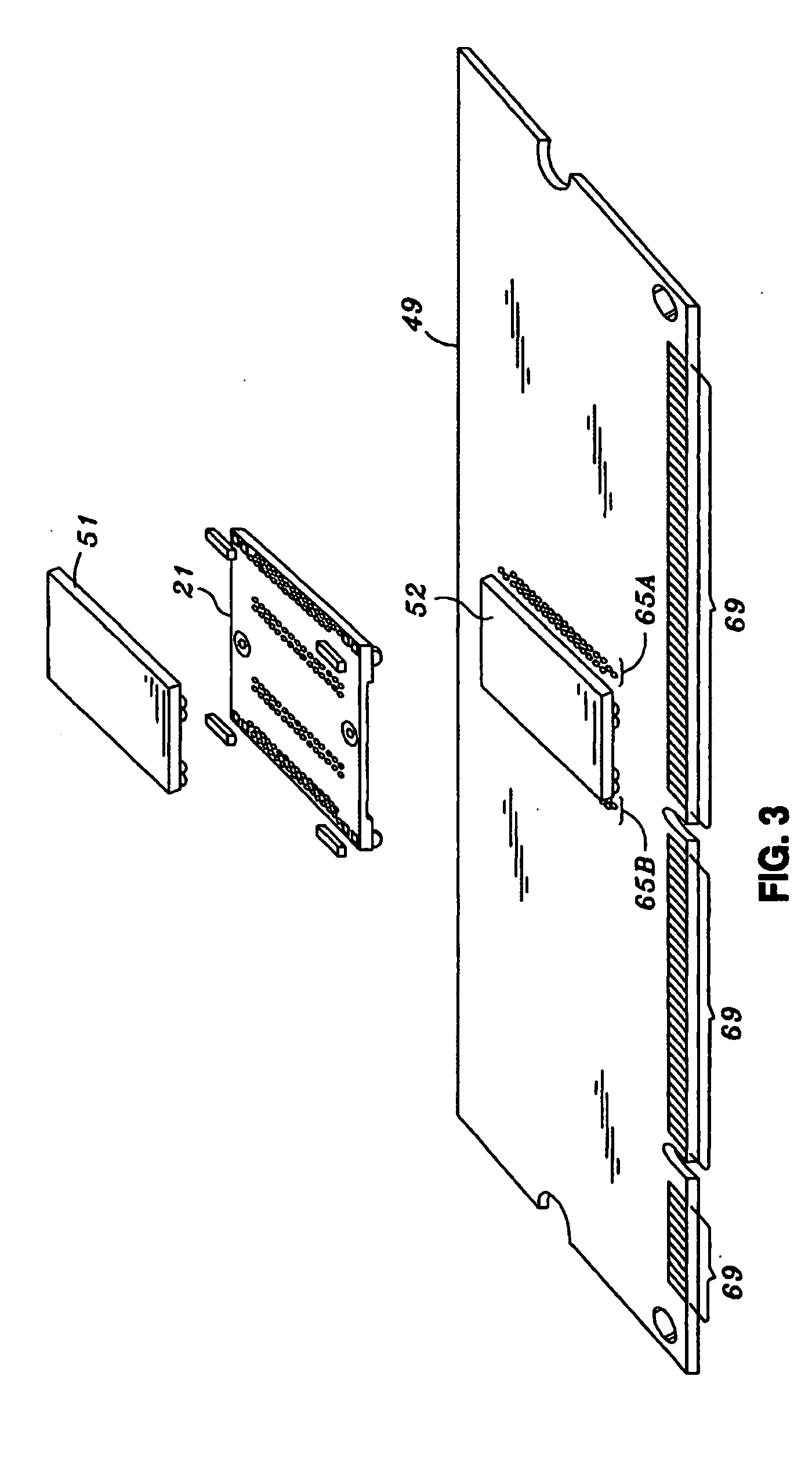
[0044] The present invention provides a chip carrier that allows for the stacking or arranging in a three dimensional array of two or more chips together on a printed circuit board and the interconnection of the stacked chips into the circuitry of the board. FIG. 1 is a perspective view of a preferred embodiment of the chip carrier 21 of the present invention. Chip carrier 21 has top platform 23 and two side struts 25 and 27. An array of BGA pads 29A and 29B on the top of platform 23 are positioned to receive an IC chip that connects by means of a BGA pad array. As will be discussed and illustrated below, pads 29A and 29B connect to vias that descend into platform 23 and then connect by conduction lines running laterally to vias in struts 25 and 27. Top exposed portions 33 of each of the vias in struts 25 and 27 can be seen at the top edge of platform 23 above each strut, 25 and 27. As will be described and illustrated below each of the vias in strut 25 and 27 descent down through s...


PUM


Abstract

An apparatus and method is disclosed that allows for the arranging in a three dimensional array semiconductor chips on a circuit board. A unique chip carrier is disclosed on which any IC chip can be positioned on above the other on a circuit board. Additionally, the carrier allows for the testing of IC chips on the carrier and underneath it without having to remove the carrier and chips from the system even if they are of the BGA or CSP type. The carrier includes exposed test points to allow an on site test.

Description

CROSS REFERENCE TO RELATED APPLICATIONS [0001] The present application is a continuation of, and claims priority under 35 U.S.C. § 120 to, U.S. application Ser. No. 10 / 371,061, filed 21 Feb. 2003, which claims priority under 35 U.S.C. § 119(e) to U.S. provisional application Ser. No. 60 / 360,473, filed 26 Feb. 2002, and is a continuation-in-part of, and claims priority under 35 U.S.C. § 120 to, U.S. application Ser. No. 09 / 688,499, filed 16 Oct. 2000, now U.S. Pat. No. 6,545,868, issued 8 Apr. 2003, which is a continuation-in-part of, and claims priority under 35 U.S.C. § 120 to, U.S. application Ser. No. 09 / 524,324, filed 13 Mar. 2000, now U.S. Pat. No. 6,487,078, issued 26 Nov. 2002, which are incorporated herein by reference.[0002] A portion of the disclosure of this patent document contains material that is subject to copyright protection. The copyright owner has no objection to facsimile reproduction by any one of the patent disclosure, as it appears in the Patent and Trademark ...

Claims


Application Information

Patent Timeline
Patent Type & Authority Applications(United States)
IPC IPC(8): H05K1/11H01L25/065H05K1/00H05K1/02H05K1/14H05K1/18H05K3/34
CPCH01L25/0652H01L2225/06572H01L2224/16H01L2924/01078H01L2924/15331H01L2924/3011H05K1/0231H05K1/0268H05K1/0298H05K1/141H05K1/144H05K1/183H05K3/3436H05K2201/049H05K2201/09036H05K2201/09954H05K2201/10515H05K2201/10734H05K2203/1572H01L2225/0652H01L2225/06517H01L25/0657H05K7/12H05K1/14
Inventor KLEDZIK, KENNETH J.ENGLE, JASON C.
Owner LEGACY ELECTRONICS INC
Why Eureka
Try Eureka