Integrated circuit comprising a photodiode of the floating substrate type and corresponding fabrication process

Inactive Publication Date: 2006-11-16
STMICROELECTRONICS SRL
View PDF13 Cites 21 Cited by
  • Summary
  • Abstract
  • Description
  • Claims
  • Application Information

AI Technical Summary

Benefits of technology

[0031] The advantage of varying the doping of the contact region i

Problems solved by technology

In addition, in order to direct the charges into the photodiode bulk during the reset phase, it is necessary to use relatively high voltages and also th

Method used


Image

  • Integrated circuit comprising a photodiode of the floating substrate type and corresponding fabrication process
  • Integrated circuit comprising a photodiode of the floating substrate type and corresponding fabrication process
  • Integrated circuit comprising a photodiode of the floating substrate type and corresponding fabrication process

Examples


Embodiment Construction

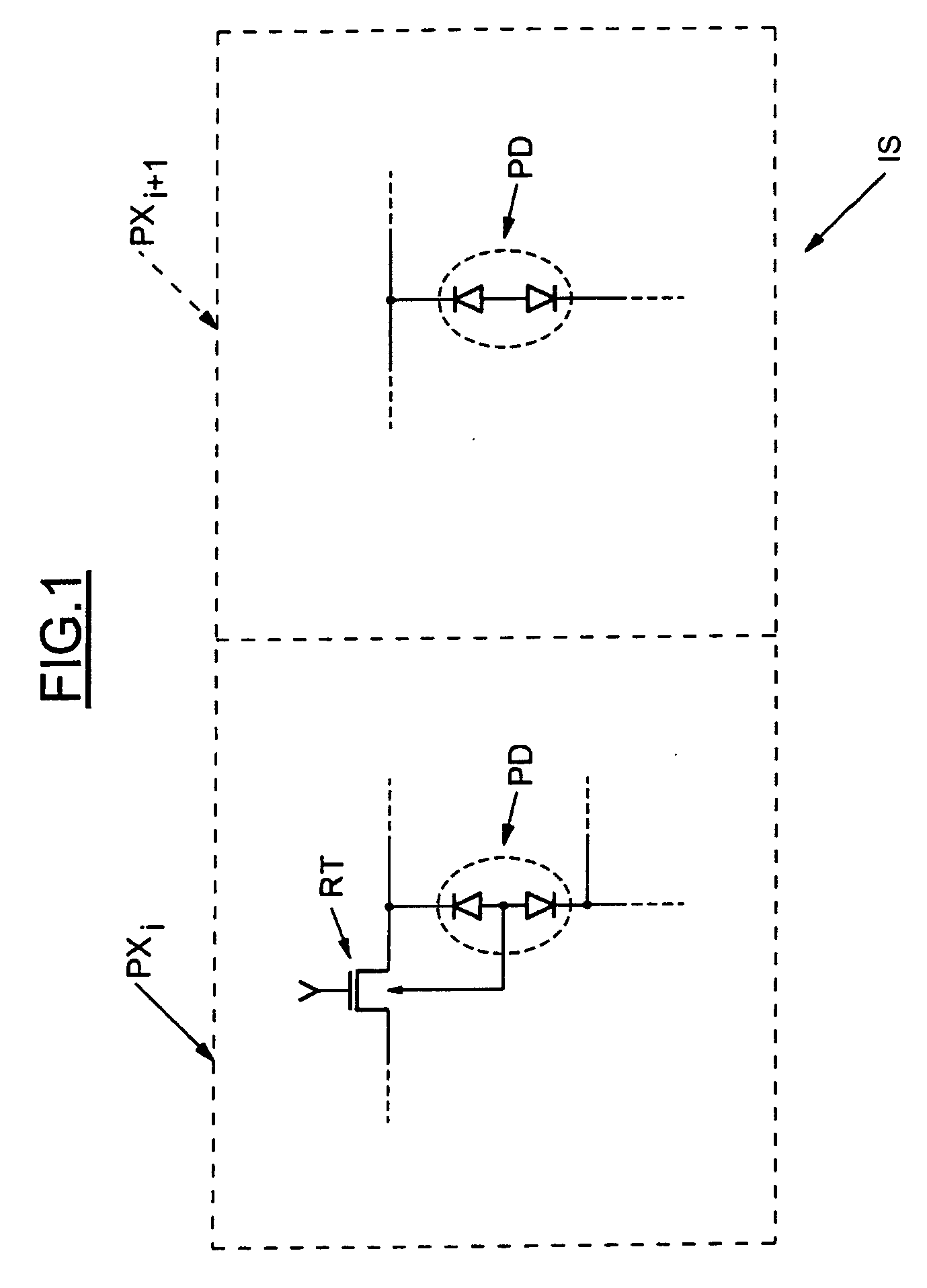
[0053] In FIG. 1, the reference IS denotes in general an image sensor formed from a matrix of cells (or pixels) PXi, each comprising a photodiode PD and a read transistor RT connected to the photodiode PD. Each cell PXi may include additional control means connected to the read transistor RT, for example a reset transistor, a select transistor and a follower transistor.

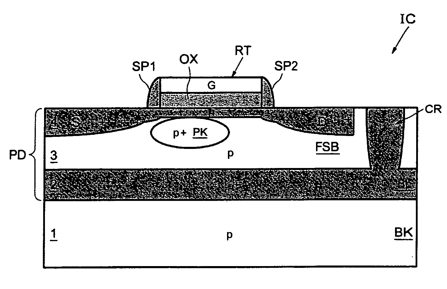
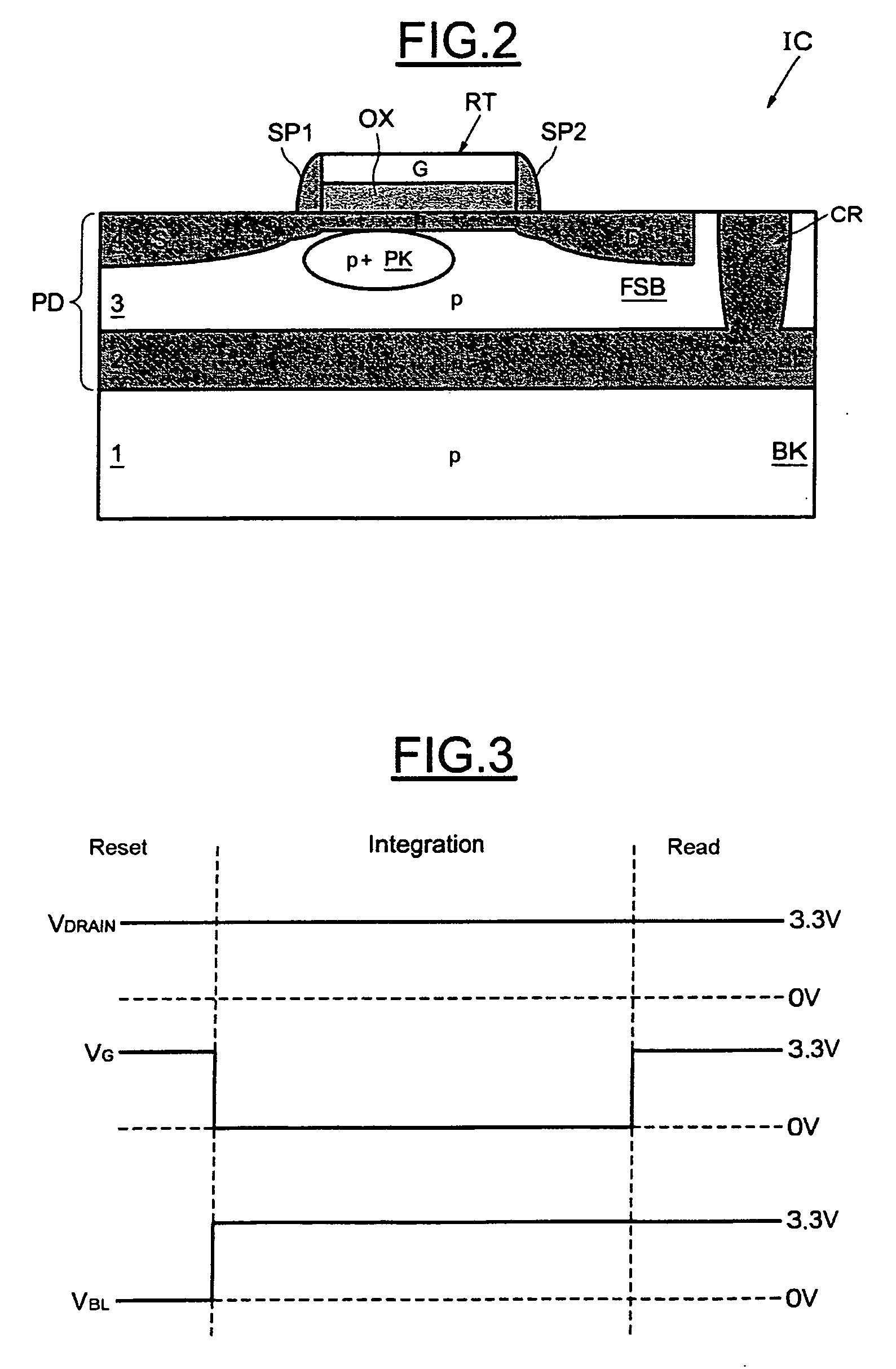
[0054]FIG. 2 shows in greater detail the semiconductor structure of the photodiode PD of a cell PXi.

[0055] The reference IC denotes an integrated circuit according to a first embodiment of the invention, comprising the photodiode PD formed on a layer 1 of substrate or bulk BK, which here is p-doped and constitutes the support for the integrated circuit.

[0056] The integrated circuit IC also includes the read transistor RT for a cell PXi.

[0057] The photodiode PD includes a stack of semiconductor layers 2, 3 and 4 that are located above the bulk layer 1.

[0058] This stack comprises a semiconductor layer 2, here n dop...


PUM


Abstract

An integrated circuit includes at least one photodiode associated with a read transistor. The photodiode is formed from a stack of three semiconductor layers comprising a buried layer, an floating substrate layer and an upper layer. The drain region and/or the source region of the transistor are incorporated within the upper layer. The buried layer is electrically isolated from the upper layer so as to allow the buried layer to be biased independently of the upper layer.

Description

PRIORITY CLAIM [0001] The present application claims priority from French Application for Patent No. 05 04835 filed May 13, 2005, the disclosure of which is hereby incorporated by reference. BACKGROUND OF THE INVENTION [0002] 1. Technical Field of the Invention [0003] The present invention relates to microelectronics, and especially to integrated circuits comprising photodiodes of the floating substrate type. [0004] 2. Description of Related Art [0005] Image sensors based on semiconductor components advantageously rely on the principle of photons being converted into electron / hole pairs in silicon. More precisely, the charges created in photosensitive regions are stored in the photodiode and are then read by an electronic system. This electronic system, which controls the photodiode, comprises in particular a read transistor for converting the charges stored in the photodiode into an electrical quantity. [0006] The present invention applies advantageously but without limitation to C...

Claims


Application Information

Patent Timeline
IPC IPC(8): H01L27/148
CPCH01L27/14609H01L27/1443
Inventor ROY, FRANCOISTOURNIER, ARNAUD
Owner STMICROELECTRONICS SRL
Why Eureka
Try Eureka