Oscillator and an integrated circuit

a technology of integrated circuits and oscillators, which is applied in the direction of oscillator generators, electrical equipment, etc., can solve the problems of noise and interference injection into the core of the oscillator, providing an interference path into the circuit, and severe grounding of the oscillator, etc., and achieves the effect of easy bias

Active Publication Date: 2006-03-09
TELEFON AB LM ERICSSON (PUBL)
View PDF2 Cites 10 Cited by
  • Summary
  • Abstract
  • Description
  • Claims
  • Application Information

AI Technical Summary

Benefits of technology

[0023] In expedient embodiments the transistors are of the Bipolar Junction Transistor (BJT) type. Since BJT transistors do not have the so-called back-gate effect that MOS transistors have, this source to substrate interference path is avoided.
[0024] In a preferred embodiment, the first, second, and third of said interconnections consist of a pair of collector-type terminals, base-type terminals, and emitter-type terminals, respectively; thereby configuring the balanced oscillator circuit with a dual common-collector transistor coupling. This preferred embodiment is advantageous in that it is relatively easy to bias e.g. by a simple resistor subcircuit. Additionally, since the collector is connected to the ground reference, the substrate portion that constitutes the collector of the transistors can provide shielding of the base and emitter of the transistors, thus further protecting the oscillator from noise signals.

Problems solved by technology

This gain cell uses single-ended signals, and as a consequence, grounding of the oscillator is a severe problem for large digital chips.
This lack of sufficient grounding may result in noise and interference injection into the core of the oscillator.
Similarly, the integrated circuit substrate will not be connected directly to the resonator ground, thereby also providing an interference path into the circuit.
The above single-ended oscillators all suffer from not being sufficiently robust to substrate interference.
However, a drawback of this and other oscillators is a lack of robustness to the so-called substrate interference, which may originate in e.g. circuits on the same substrate involving intense digital switching, or other strong interference induced at the oscillator nodes, e.g. from another on-chip RF oscillator.
This imperfect performance results in small variations in the oscillation frequency, so called frequency shifts.
The GSM / GPRS requirements are more stringent than 1 ppm and, generally, this oscillator does not perform well enough with respect to the GSM / GPRS requirements.
As stated above, an integrated oscillator is prone to pick up substrate interference.
Furthermore, the drain has a parallel-plate capacitance to the substrate and this path may also cause noise injection.

Method used


Image

  • Oscillator and an integrated circuit
  • Oscillator and an integrated circuit
  • Oscillator and an integrated circuit

Examples


Embodiment Construction

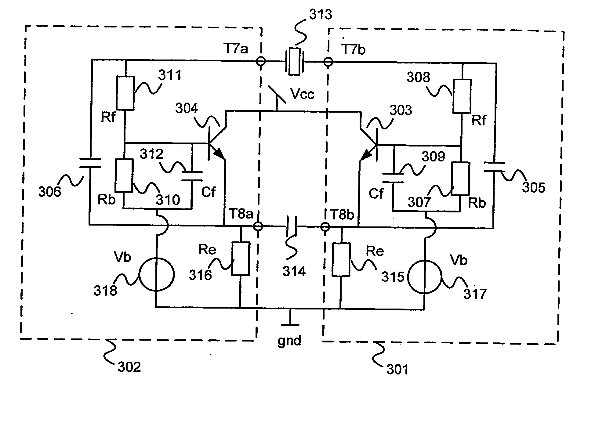
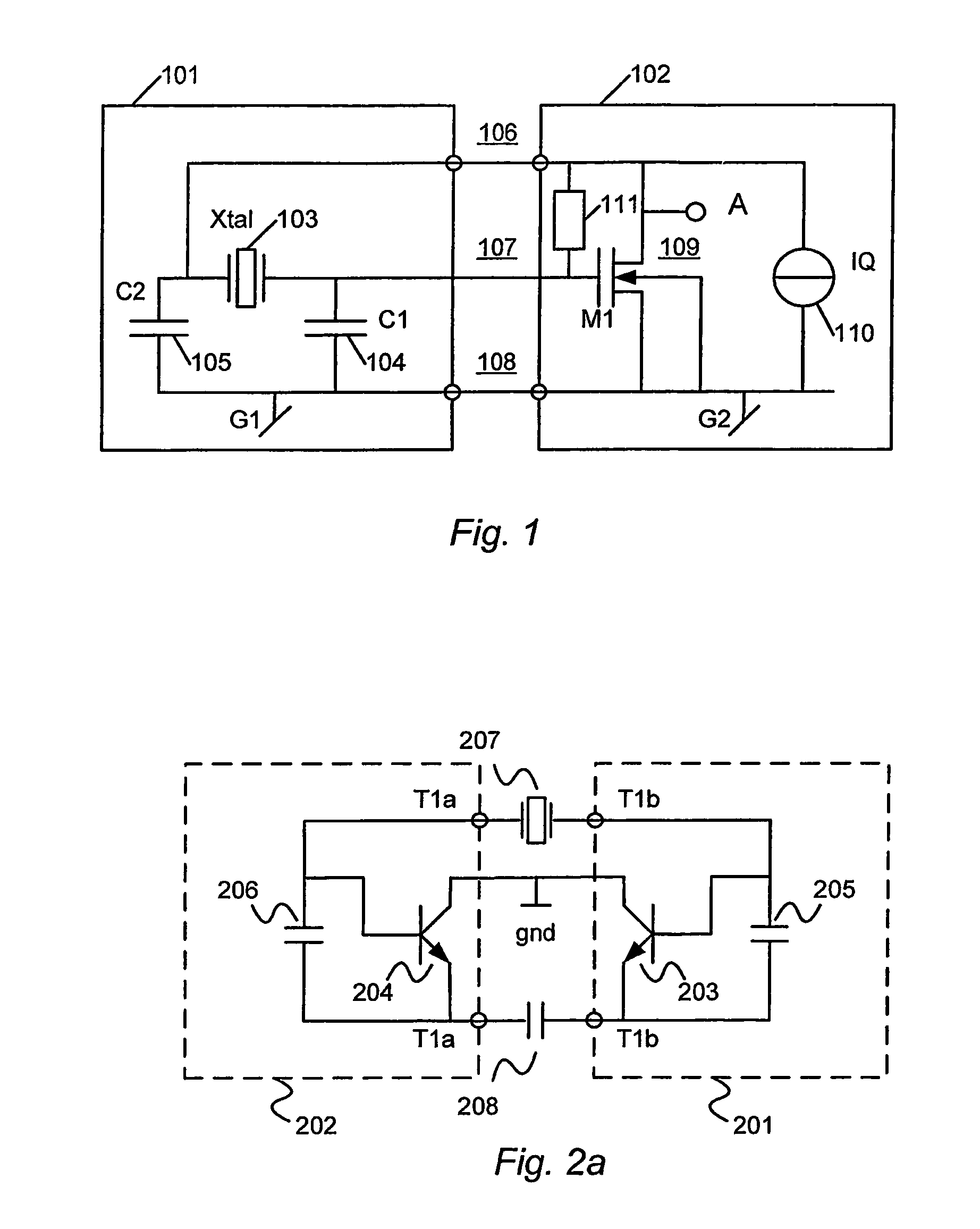
[0047]FIG. 1 shows a single-ended crystal oscillator. The oscillator circuit is illustrated to comprise a first and a second subcircuit. The first subcircuit 101 is typically implemented by means of passive components mounted on a printed circuit board (PCB), whereas the second subcircuit 102 is implemented on a substrate in an integrated circuit (IC) component that is mounted on the PCB.

[0048] The first subcircuit 101 comprises an oscillating device in the form of a crystal (Xtal) 103 for instance with a nominal oscillating frequency in the range of 10-40 MHz. The crystal is electrically connected to the second subcircuit 102 by means of two connectors 106 and 107.

[0049] At frequencies about the nominal series resonance frequency the crystal has relatively low impedance. However, at frequencies below and above the series resonance frequency the crystal has relatively high impedance. Thus, below and especially above the nominal frequency an oscillating signal across the crystal wi...


PUM


Abstract

A balanced crystal oscillator circuit comprising: a piezoelectric element Xtal (207; 215; 222,221; 313); a first oscillator subcircuit (202; 210; 218; 302) incorporating a transistor (204;212;220;304); and a second oscillator subcircuit (201;209;217;301) incorporating a transistor (203; 211; 219; 303); wherein the transistors each have different types of transistor terminals (C,B,E; D;G;S), and wherein the oscillator subcircuits are configured with at least three interconnections. Each interconnection comprise a pair of like type of transistor terminals; wherein a first of said interconnections constitutes a connection to a ground reference (gnd); a second of said interconnections is via a first resonator element (207;215;223;313); and a third of said interconnections is via a second resonator element (208;216;224;314); said first and second circuits are arranged to interact by means of said first and second resonator elements to form a balanced oscillator signal. A dual common base or a dual common collector configuration is preferred.

Description

TECHNICAL FIELD [0001] This invention relates to a balanced crystal oscillator circuit comprising: a piezoelectric element; a first oscillator subcircuit incorporating a transistor; and a second oscillator subcircuit incorporating a transistor; wherein the transistors each have different types of transistor terminals, and wherein the oscillator subcircuits are configured with at least three interconnections. BACKGROUND OF THE INVENTION [0002] A balanced crystal oscillator circuit can be employed in various electronic circuits. However, a special field of application is within communications equipment—especially telecommunications equipment—wherein frequency references are generated or synthesized as periodic signals for modulators, demodulators, up- and down frequency converters, for timing circuits etc. Typically, the periodic signals are square-wave signals. [0003] The periodic signals have a fundamental frequency and are generated by a so-called frequency synthesizer, which provi...

Claims


Application Information

Patent Timeline
Patent Type & Authority Applications(United States)
IPC IPC(8): H03B5/32H03B5/36
CPCH03B5/364H03B5/36H03B5/32
Inventor MATTISSON, SVEN
Owner TELEFON AB LM ERICSSON (PUBL)
Why Eureka
Try Eureka