Integrated circuit comprising at least one capacitor and process for forming the capacitor

a technology of integrated circuits and capacitors, which is applied in the direction of solid-state devices, basic electric elements, electric devices, etc., can solve the problems of large area occupied by capacitors, high cost, and considerable debonding

Active Publication Date: 2006-11-16
STMICROELECTRONICS SRL +1
View PDF15 Cites 12 Cited by
  • Summary
  • Abstract
  • Description
  • Claims
  • Application Information

AI Technical Summary

Benefits of technology

[0008] It is possible to remedy the foregoing and other drawbacks by forming the capacitor in the trench so as to leave a part of the trench behind a

Problems solved by technology

In integrated circuits, and especially radiofrequency integrated circuits, the capacitors occupy a very large area, hence a high cost.
However, it is found that, with this process, the mechanical stresses on the materials used to form the capacitors cause considerable debonding, espe

Method used


Image

  • Integrated circuit comprising at least one capacitor and process for forming the capacitor
  • Integrated circuit comprising at least one capacitor and process for forming the capacitor
  • Integrated circuit comprising at least one capacitor and process for forming the capacitor

Examples


Embodiment Construction

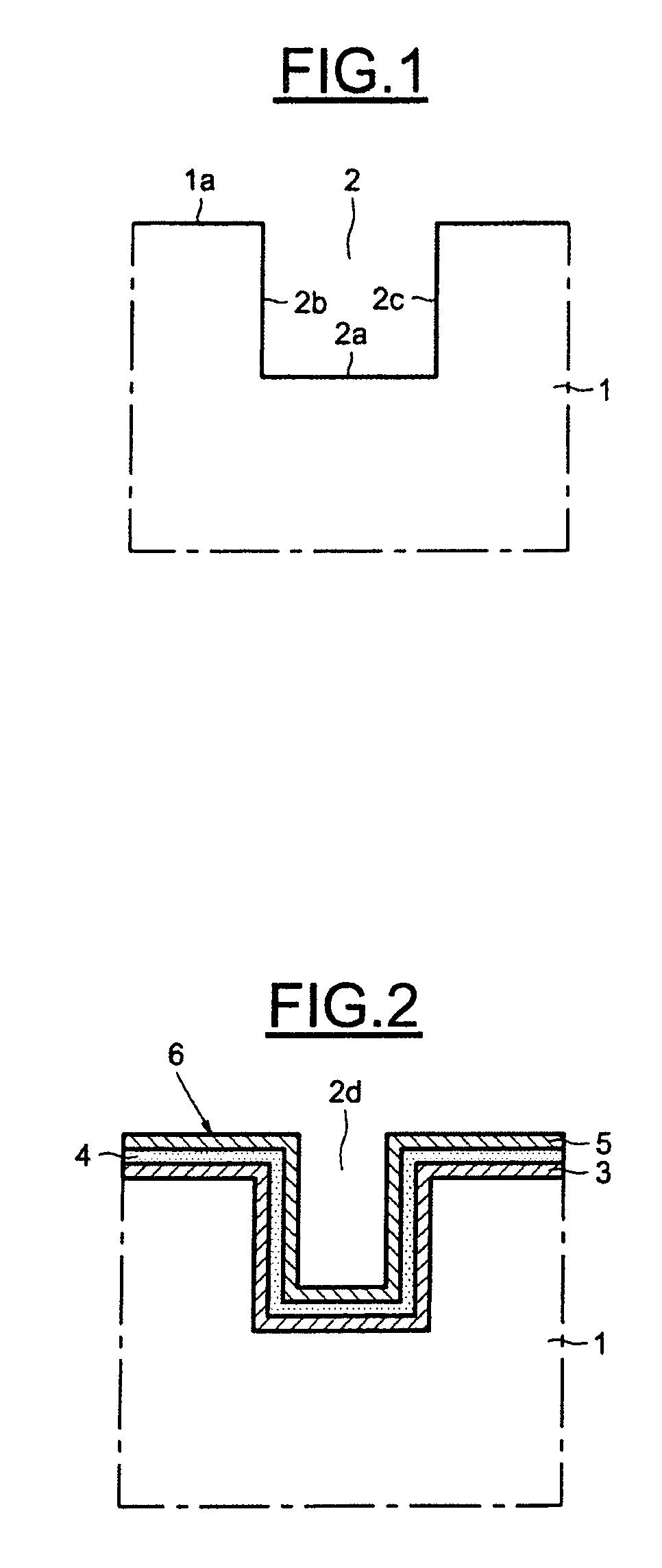
[0030] [28] FIGS. 1 to 13 are cross-sectional views of the integrated circuit at various steps in the process for forming the capacitor according to the invention.

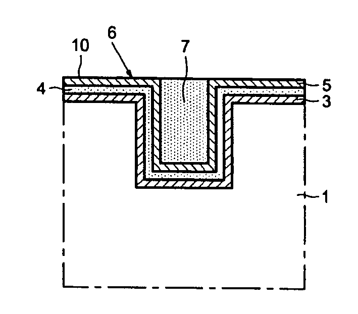
[0031]FIG. 1 shows a layer 1, which may be made of silicon, glass, SiO2 or any other insulating material. The layer 1 is typically a substrate with a planar upper surface 1a. A rectangular trench 2 is etched into the layer 1, for example by dry fluorine etching. The trench 2 has a bottom 2a parallel to the planar upper surface 1a of the layer 1, and also parallel edges 2b and 2c of length generally greater than that of the bottom 2a. The depth of the trench 2 is generally between 1 and 200 μm. For example, it is possible to form trenches with a depth of between 1 and 10 μm in an interconnect region or a depth of between 10 and 100 μm in a substrate.

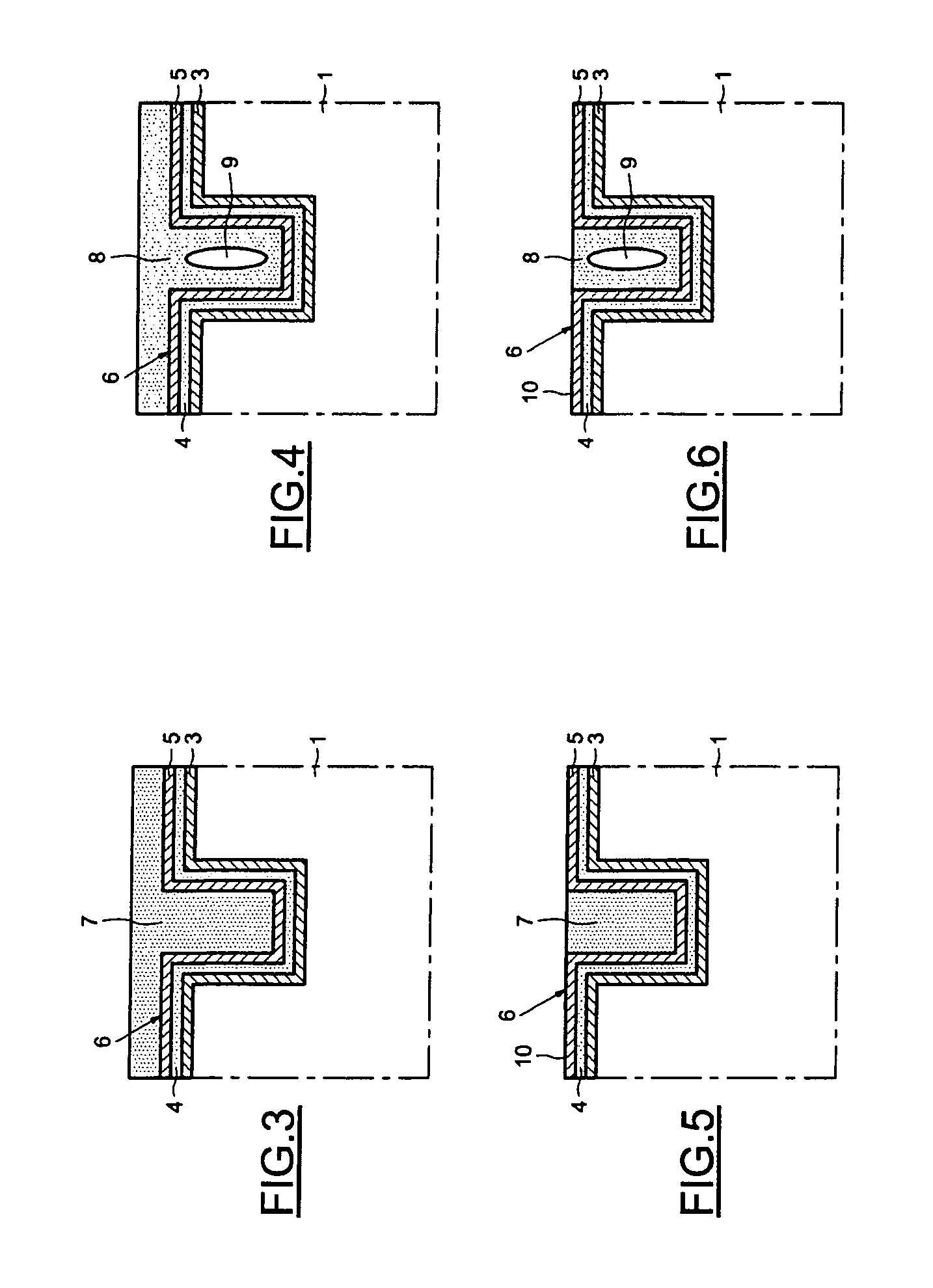
[0032] Next, a capacitor 6 is formed (FIG. 2) by depositing, in succession, a first electrode, in the form of a layer 3, a dielectric layer 4 and a second electrode in the for...


PUM


Abstract

An integrated circuit includes at least one capacitor that is formed on a layer provided with at least one first trench. The capacitor, which is provided with a dielectric layer that separates two electrodes, conforms to the shape of the first trench, but leaves a part of the first trench unfilled. A material capable of absorbing stresses associated with the displacements of the walls of the trench is placed in the trench to fill the part of the first trench. A second trench is formed at least partly surrounding the first trench. This second trench is also at least partly filled with a material capable of absorbing stresses associated with the displacements of the walls of the second trench. A void may be included in the stress absorbing material which fills either of the first or second trenches.

Description

PRIORITY CLAIM [0001] The present application claims priority from French Application for Patent No. 05 04536 filed May 4, 2005, the disclosure of which is hereby incorporated by reference. BACKGROUND OF THE INVENTION [0002] 1. Technical Field of the Invention [0003] The present invention relates to the formation of capacitors within an integrated circuit. [0004] 2. Description of Related Art [0005] In integrated circuits, and especially radiofrequency integrated circuits, the capacitors occupy a very large area, hence a high cost. Thus, there is a need to increase the capacitance per unit area of these capacitors, while still maintaining the performance requirements for radiofrequency applications. [0006] To do this, it is known to form capacitors in three dimensions in trenches or wells, thereby enabling the surface density of the electrodes to be increased. [0007] However, it is found that, with this process, the mechanical stresses on the materials used to form the capacitors ca...

Claims


Application Information

Patent Timeline
IPC IPC(8): H01L29/00
CPCH01L21/31612H01L21/31633H01L29/66181H01L28/91H01L27/0805H01L21/02126H01L21/02164
Inventor GIRAUDIN, JEAN-CHRISTOPHEFIORI, VINCENTDELPECH, PHILIPPE
Owner STMICROELECTRONICS SRL
Why Eureka
Try Eureka