Panel for electro-optical apparatus, method of manufacture thereof, electro-optical apparatus and electronic apparatus

a technology of electro-optical apparatus and electro-optical apparatus, which is applied in the direction of identification means, instruments, and the formation of printed elements, can solve problems such as stress and heat deformation, and achieve the effect of excellent display quality

Inactive Publication Date: 2005-09-22
138 EAST LCD ADVANCEMENTS LTD
View PDF7 Cites 4 Cited by
  • Summary
  • Abstract
  • Description
  • Claims
  • Application Information

AI Technical Summary

Benefits of technology

[0016] According to this type of structure, because convex portions that are made of resin are provided on a substrate, it is not necessary to form electrolytic Au bumps, which are high-cost, conductive protruding portions, on connection terminals of an electronic component that is being packaged on the substrate. In addition, when packaging the electronic component on the substrate, there are cases in which heat deformation such as stress is generated in the substrate or electronic component by heating or pressure. However, according to this type of structure, because convex portions that are made of resin are provided on the substrate, when the electronic component is being packaged on the substrate, it is possible to absorb stress from the electronic component or panel. As a result, malfunctions in the packaging of the electronic component can be avoided.
[0042] According to this type of structure, an electronic apparatus can be provided that has an excellent display quality.

Problems solved by technology

In addition, when packaging the electronic component on the substrate, there are cases in which heat deformation such as stress is generated in the substrate or electronic component by heating or pressure.
Moreover, according to this, it is also unnecessary to provide a conductive layer that covers the surfaces of the convex portions, and to electrically connect this conductive layer to each wire.

Method used


Image

  • Panel for electro-optical apparatus, method of manufacture thereof, electro-optical apparatus and electronic apparatus
  • Panel for electro-optical apparatus, method of manufacture thereof, electro-optical apparatus and electronic apparatus
  • Panel for electro-optical apparatus, method of manufacture thereof, electro-optical apparatus and electronic apparatus

Examples


first embodiment

(First Embodiment)

(Structure of a Liquid Crystal Panel)

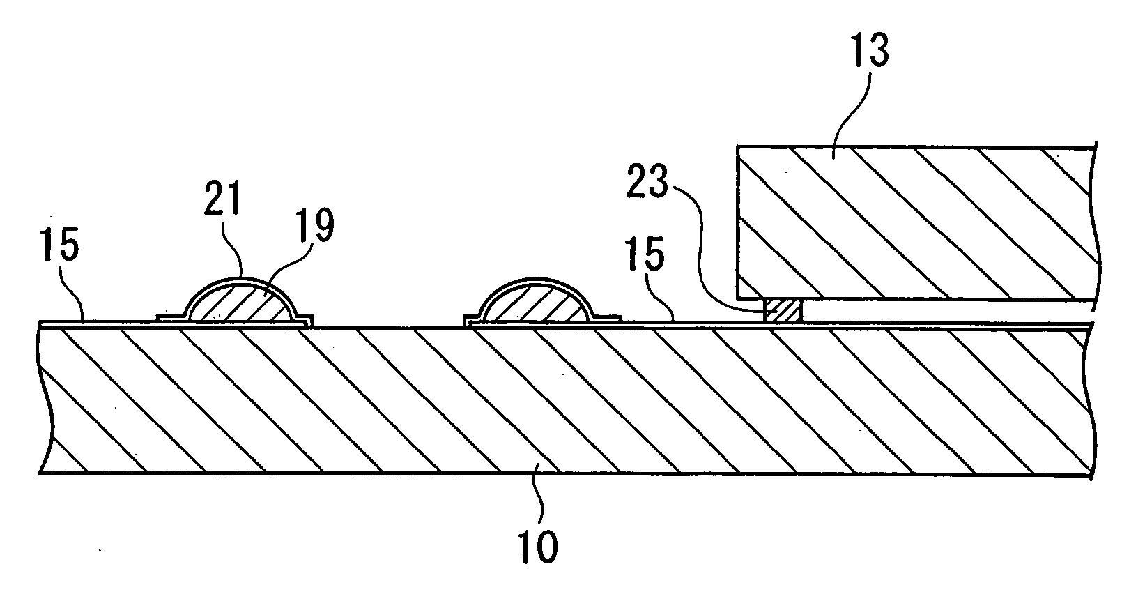
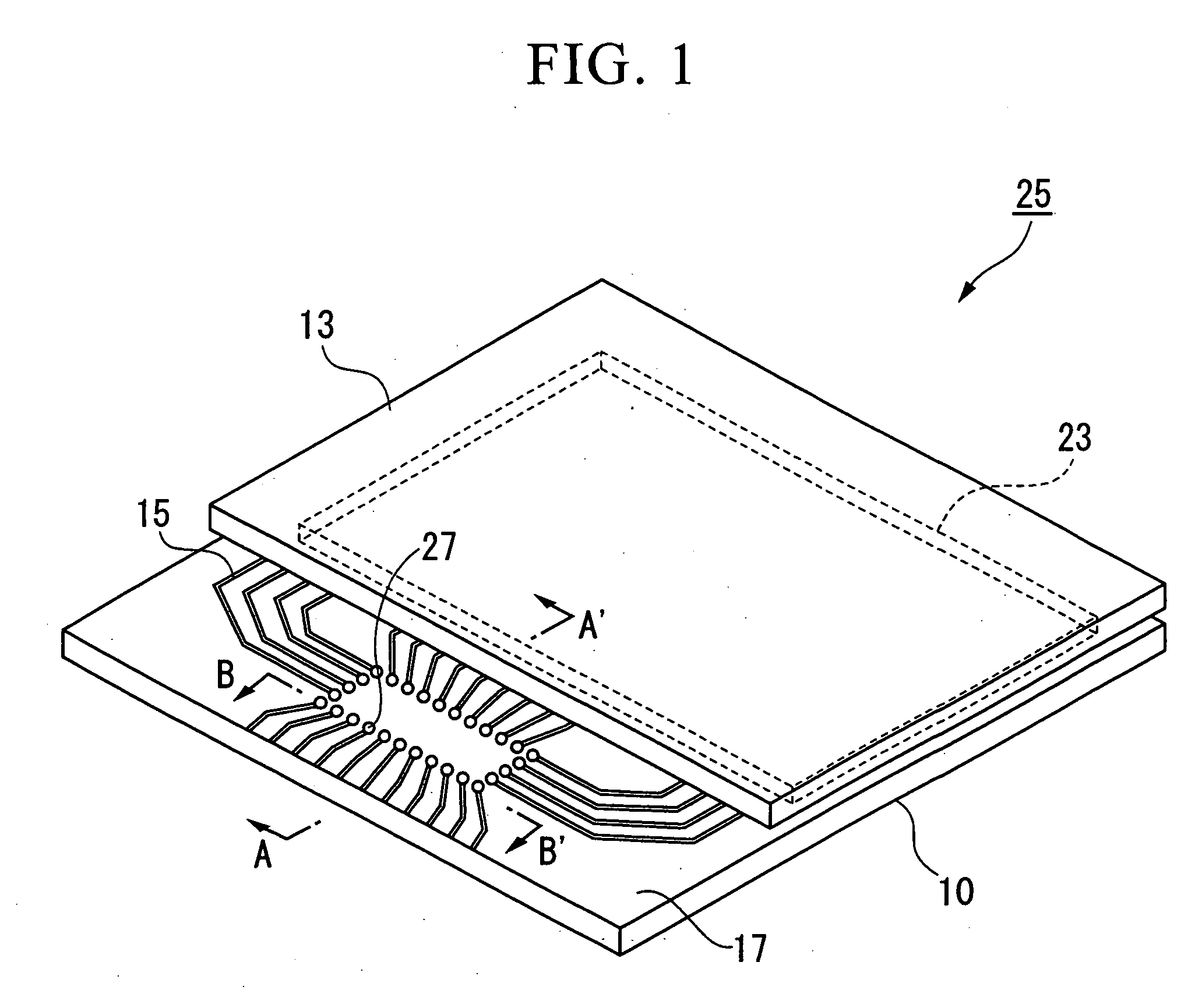
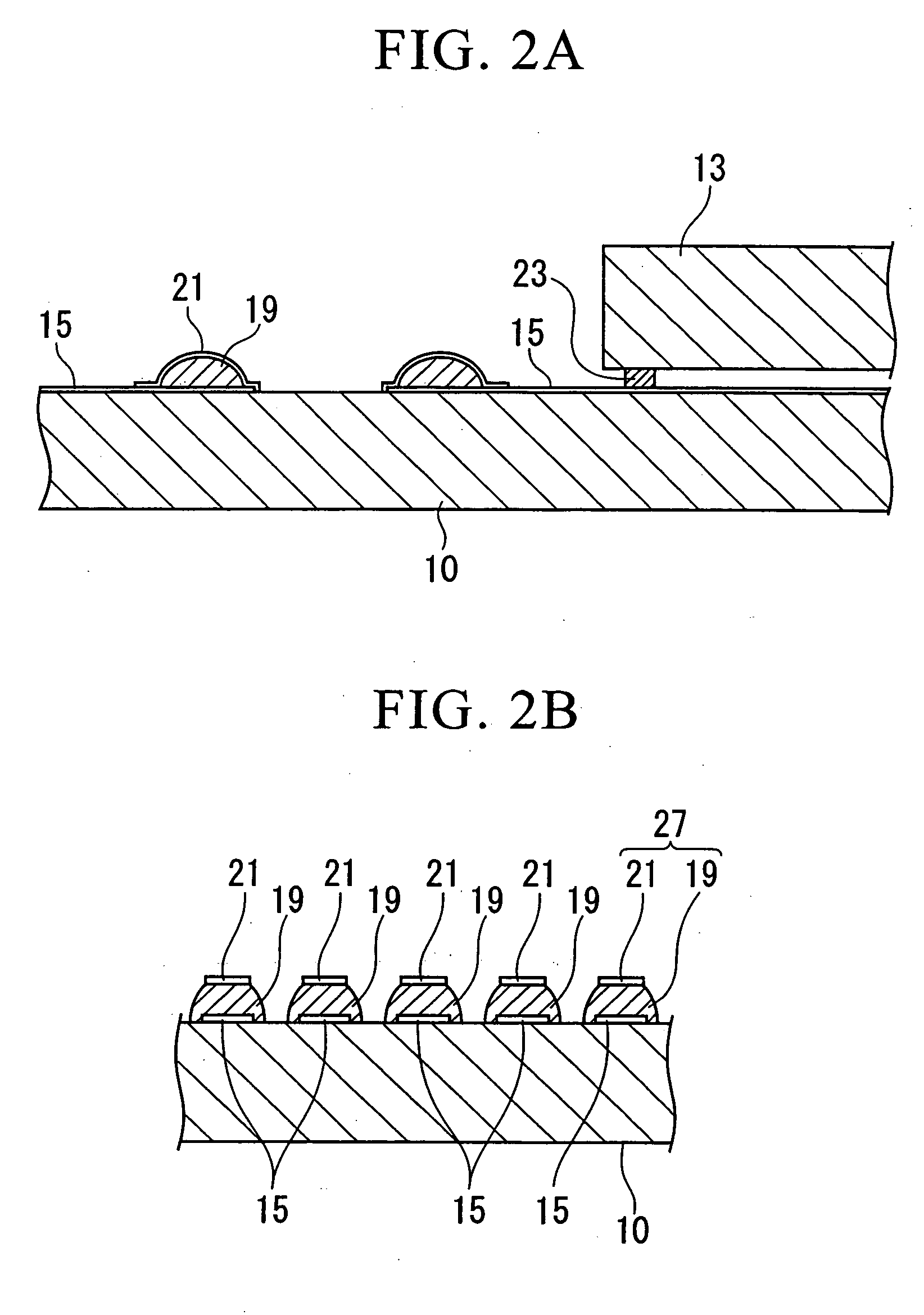
[0061]FIG. 1 is a perspective view showing the schematic structure of a liquid crystal panel 25 (i.e., a panel for an electro-optical apparatus) of the present embodiment. In the liquid crystal panel 25, a first substrate 10 (i.e., a substrate) and a second substrate 13 are bonded by an ultraviolet light-cured sealing material 23. Liquid crystal is sealed and held inside an area surrounded by this sealing material 23. In addition, the liquid crystal panel 25 is provided with a plurality of wires 15 that are formed in a predetermined pattern on the first substrate 10, convex portions 19 that are formed on top of the wires 15, and conductive layers 21 that are formed on top of the convex portions 19. Furthermore, illumination devices such as backlights and other accessory equipment are also provided for the liquid crystal panel 25.

[0062] The first substrate 10 is formed from soda glass and a transparent electrode layer is forme...

second embodiment

(Second Embodiment)

[0100] In the above described the first embodiment, thin films are manufactured using a sputtering method, and these manufactured thin films are formed into wires 15, convex portions 19, and conductive layers 21 in a predetermined pattern using a photolithographic method. In contrast to this, in the present embodiment, instead of the above described formation method that is based on a photolithographic method, the wires 15, convex portions 19, and conductive layers 21 are formed using an inkjet method. A description is given below in detail of the structure of an inkjet apparatus and of a method of forming the wires 15, convex portions 19, and conductive layers 21. Note that because the painting step in which the sealing material 23 is painted on the first substrate 10, the preliminary curing step to cure the painted sealing material 23, the liquid crystal placement step in which the liquid crystal 25 is placed in an area on the substrate that is surrounded by the...

third embodiment

(Third Embodiment)

[0129] In the embodiments described above, the conductive layers 21 are formed on the surface of the convex portions 19, which is composed of resin, and these conductive layers 21 are electrically connected to the wires 15. In contrast to this, in the present embodiment, the conductive layers 21 are formed on the surface of the convex portions 19 so as to cover the wires 15.

[0130]FIG. 13A is a cross-sectional view taken along the line A-A′ in FIG. 1 when the wires 15 are formed so as to cover a portion of the surface of the convex portions 19. FIG. 13B is a cross-sectional view taken along the line B-B′ in FIG. 1. The wires 15 that are provided on the first substrate 10 are formed on each of the convex portions 19, which are formed individually on the first substrate 10, so as to cover the surfaces of the convex portions 19. Namely, in the present embodiment, the wires 15 are also provided with the functions of the conductive layers 21. In this case, a convex port...


PUM

PropertyMeasurementUnit
heightaaaaaaaaaa
thicknessaaaaaaaaaa
thicknessaaaaaaaaaa

Abstract

A panel for an electro-optical apparatus, includes a substrate, a plurality of wires formed on the substrate, convex portions formed from resin and provided either on the plurality of wires or on the substrate, conductive layers provided so as to cover at least a portion of the surfaces of the convex portions, and that are electrically connected to the respective wires, and a plurality of external connection terminals for electrically connecting electronic components, formed by the convex portions and the conductive layers.

Description

BACKGROUND OF THE INVENTION [0001] 1. Field of the Invention [0002] The present invention relates to a panel for an electro-optical apparatus, a method of manufacture thereof, an electro-optical apparatus and an electronic apparatus. [0003] Priority is claimed on Japanese Patent Application No. 2004-76323, filed Mar. 17, 2004, the contents of which are incorporated herein by reference. [0004] 2. Description of Related Art [0005] Conventionally, when packaging a semiconductor device such as a drive IC on a liquid crystal panel or the like, a method is widely used in which what are known as Au bumps are formed on the drive IC, and the drive IC is then packaged on the liquid crystal panel or the like via an adhesive agent. These Au bumps are formed by sputtering a seed layer of TiW / Au or the like on the drive IC, and then patterning the resist. Subsequently, electrolytic gold plating is coated on the resist to a height of approximately 20 μm. An anisotropic conductive film (ACF) is wid...

Claims


Application Information

Patent Timeline
Patent Type & Authority Applications(United States)
IPC IPC(8): G02F1/1345G02F1/13G02F1/1362G09F9/00H05K3/00H05K3/40
CPCG02F1/136277H05K3/0023H05K3/4007H05K2201/0367H05K2201/09909Y10T29/49126G02F1/13452G02F1/13458G02F1/1362Y10T29/49155Y10T29/4913H05K2203/013G02F1/1345
Inventor ITO, HARUKI
Owner 138 EAST LCD ADVANCEMENTS LTD
Why Eureka
Try Eureka