POP (Package-On-Package) device encapsulating soldered joints between externals leads

a technology of soldering joints and pops, which is applied in semiconductor devices, semiconductor/solid-state device details, electrical apparatus, etc., can solve the problems of soldering joints between external leads being vulnerable to breakage, and achieve the effect of avoiding electrical openness and avoiding soldering joints breaking

Inactive Publication Date: 2009-05-21
POWERTECH TECHNOLOGY
View PDF7 Cites 5 Cited by
  • Summary
  • Abstract
  • Description
  • Claims
  • Application Information

AI Technical Summary

Benefits of technology

[0005]The main purpose of the present invention is to provide a POP semiconductor device with encapsulating protection of soldered joints between the external leads to disperse the stresses exerted on the soldered joints of the external leads, to avoid the breaks of the soldering joints due to CTE mis-match of different package materials, and to avoid electrical open.

Problems solved by technology

However, the soldered joints between the external leads are vulnerable to break due to CTE mismatch leading to electrical open.

Method used


Image

  • POP (Package-On-Package) device encapsulating soldered joints between externals leads
  • POP (Package-On-Package) device encapsulating soldered joints between externals leads
  • POP (Package-On-Package) device encapsulating soldered joints between externals leads

Examples


Embodiment Construction

[0015]Please refer to the attached drawings, the present invention will be described by means of embodiment(s) below.

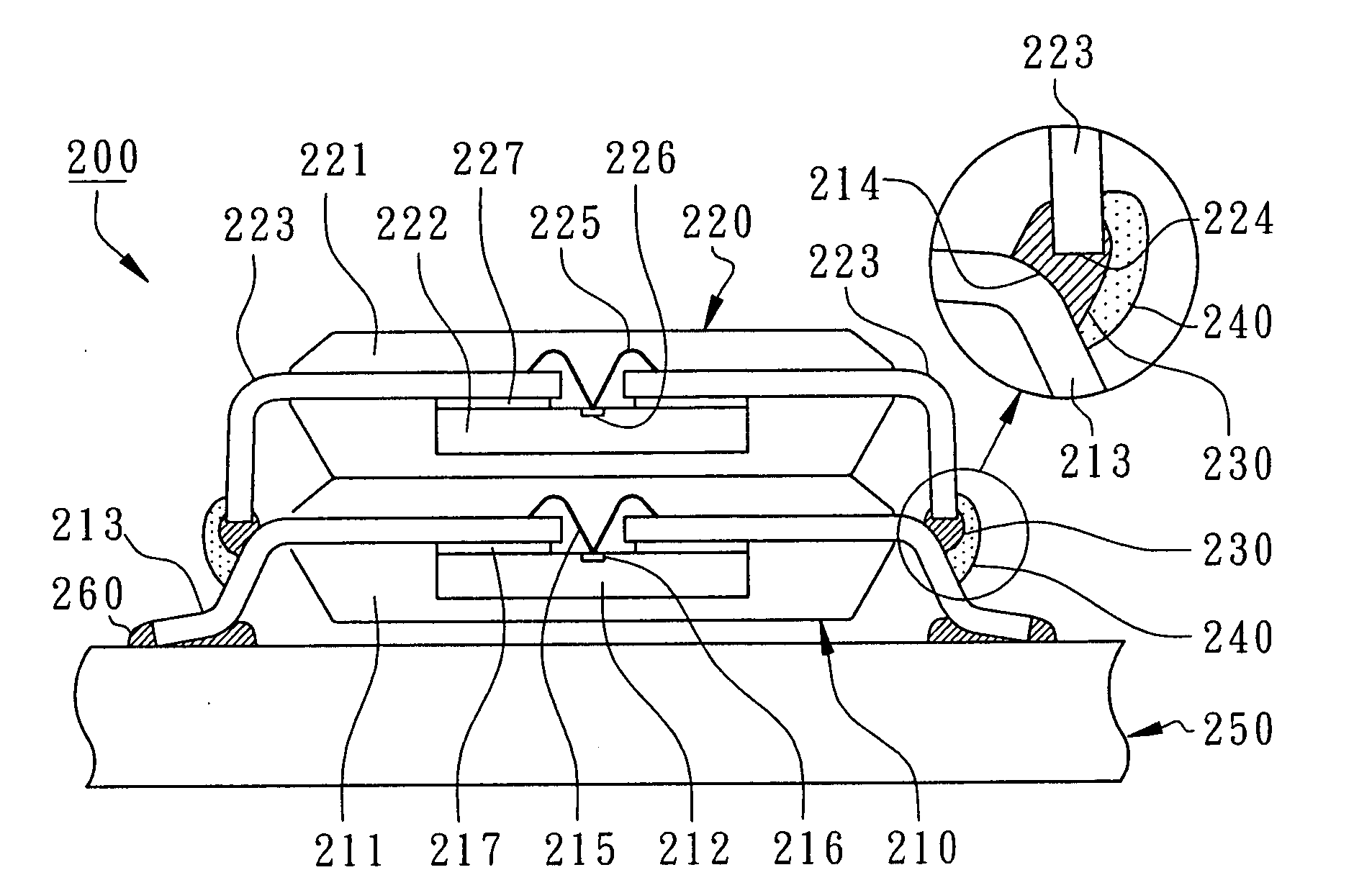
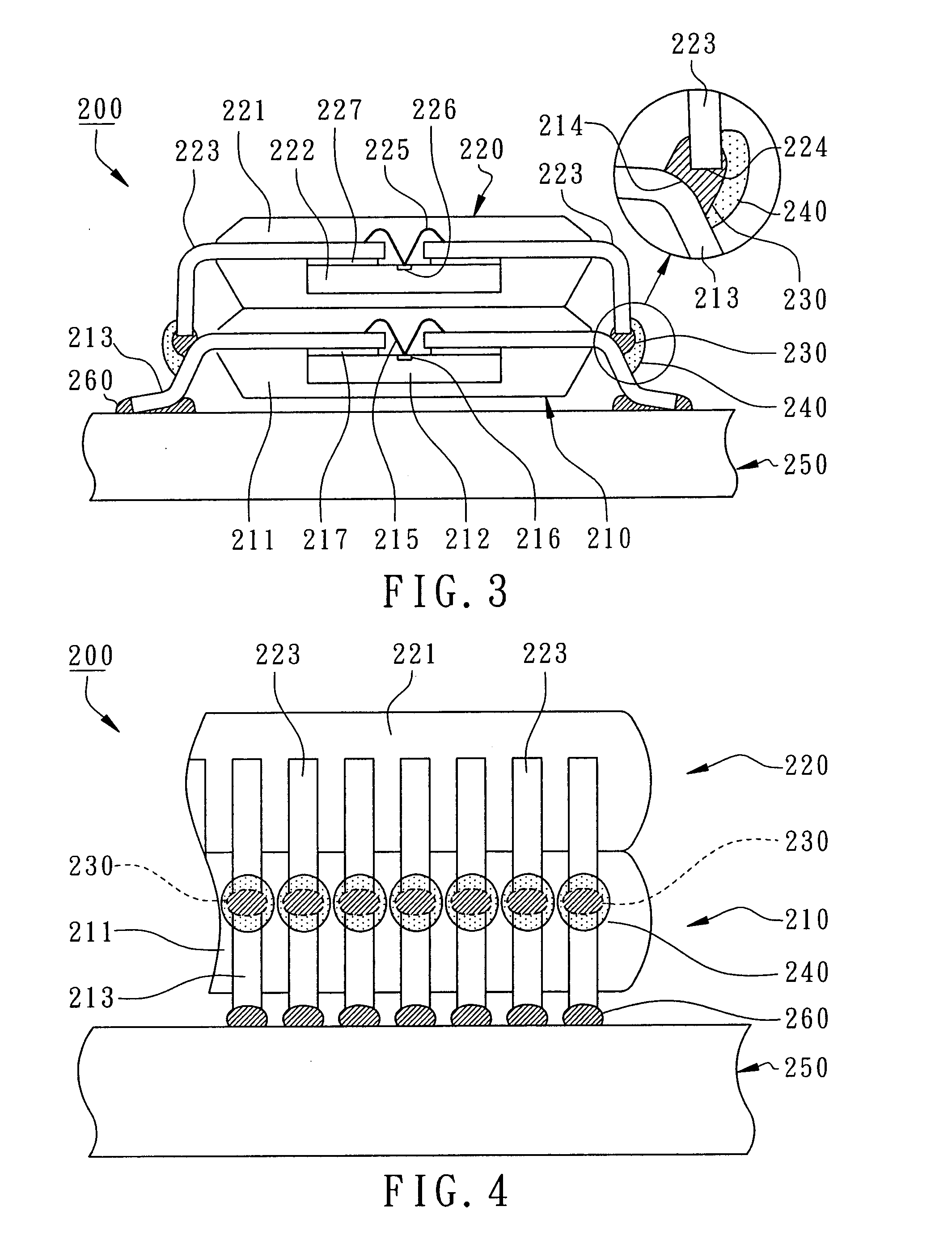
[0016]FIG. 3 and FIG. 4 are related to the first embodiment of the present invention, a POP semiconductor device 200 is provided with encapsulating protection of soldered joints between the external leads, which primarily comprises a first semiconductor package 210, at least a second semiconductor package 220, soldering materials 230, and dielectric coating 240. Therein, the first semiconductor package 210 and the second semiconductor package 220 can be single-chip package or multi-chip package. As shown in FIG. 3, in the present embodiment, the first semiconductor package 210 and the second semiconductor package 220 are single-chip TSOP's (Thin Small Outline Package). The first semiconductor package 210 includes a first encapsulant 211, a first chip 212 encapsulated inside the first encapsulant 211, and a plurality of first external leads 213 of leadframe. The first ...


PUM


Abstract

A POP (Package-On-Package) semiconductor device with encapsulating protection of soldered joints between the external leads, primarily comprises a plurality of stacked semiconductor packages and dielectric coating. Each semiconductor package includes at least a chip, a plurality of external leads of leadframe, and an encapsulant where the external leads are exposed and extended from a plurality of sides of the encapsulant. Terminals of a plurality external leads of a top semiconductor package are soldered to the soldered regions of the corresponding external leads of a bottom semiconductor package. The dielectric coating is disposed along the sides of the encapsulant of the bottom semiconductor package to connect the soldered points between the external leads and to partially or completely encapsulate the soldering materials so that the stresses between the soldered joints can be dispersed and no electrical shorts happen.

Description

FIELD OF THE INVENTION[0001]The present invention relates to a leadframe-based POP semiconductor device, especially to a leadframe-based POP semiconductor device with encapsulating protection on soldered joints between the external leads.BACKGROUND OF THE INVENTION[0002]In the recent years, more high-tech electronic devices offer lighter, thinner, and smaller features with friendly operation and multiple functions. In order to meet the requirements of smaller footprints with higher densities, 3D stacking technologies were developed such as POP (Package-On-Package) and DOD (Die-On-Die). One of the POP semiconductor devices is to vertically stack a plurality of leadframe-based semiconductor packages. The leadframe-based POP semiconductor devices using leadframes as chip carriers have the lowest overall cost where the external leads extending from the encapsulants are vertically formed and soldered together to achieve electrical connections. However, the soldered joints between the ext...

Claims


Application Information

Patent Timeline
Patent Type & Authority Applications(United States)
IPC IPC(8): H01L23/495
CPCH01L23/4951H01L2224/48091H01L24/48H01L2224/48247H01L2924/00014H01L2224/32245H01L2224/4826H01L2224/73215H01L2924/181
Inventor FAN, WEN-JENGCHEN, CHENG-PIN
Owner POWERTECH TECHNOLOGY
Why Eureka
Try Eureka