Optical waveguide device, and a travelling wave form optical modulator

a technology of optical modulator and optical waveguide substrate, which is applied in the direction of optical waveguide light guide, instruments, optics, etc., can solve the problems of increasing temperature and dc drift, and not being able to completely remove processing damage, so as to reduce the maximum stress applied and disperse the stress in the optical waveguide substrate

Inactive Publication Date: 2006-04-25
NGK INSULATORS LTD
View PDF29 Cites 20 Cited by
  • Summary
  • Abstract
  • Description
  • Claims
  • Application Information

AI Technical Summary

Benefits of technology

[0007]An object of the present invention is to provide an optical waveguide device having an optical waveguide substrate, a supporting body supporting the substrate and a joining layer joining the substrate and supporting body, so that the reliability such as temperature and DC drifts can be improved when an excessive load is applied in a reliability test such as thermal shock and temperature cycle tests.
[0010]On the contrary, according to the first aspect of the present invention, a flat plate-shaped main body having a thickness of 30 μm or smaller is used and joined with a supporting body with a joining layer, and the joining face of the supporting body is made substantially flat. It is thus possible to make the thickness of the joining layer substantially constant to remove the regions susceptible to stress concentration in the optical waveguide substrate. The maximum stress applied onto the optical waveguide substrate can be thus reduced. Further, the thickness of the main body can be reduced by polishing in an appropriate conditions to considerably reduce the processing damage and to prevent the deterioration of fracture strength at the same time.
[0012]According to the second aspect of the present invention, a flat plate-shaped main body having a thickness of 30 μm or smaller is used and joined with a supporting body with a joining layer, and the thickness of the joining layer is made 200 μm or smaller. It is thus possible to disperse the stress in the optical waveguide substrate and to reduce the maximum stress applied on the substrate.

Problems solved by technology

It has been proved that in such structure, the temperature and DC drifts may be increased when an excessive load is applied in tests for reliability such as thermal shock and thermal cycle tests.
It is, however, not possible to completely remove the processing damage according to each of the processing methods.

Method used


Image

  • Optical waveguide device, and a travelling wave form optical modulator
  • Optical waveguide device, and a travelling wave form optical modulator
  • Optical waveguide device, and a travelling wave form optical modulator

Examples


examples

Production of a Device of Example 1

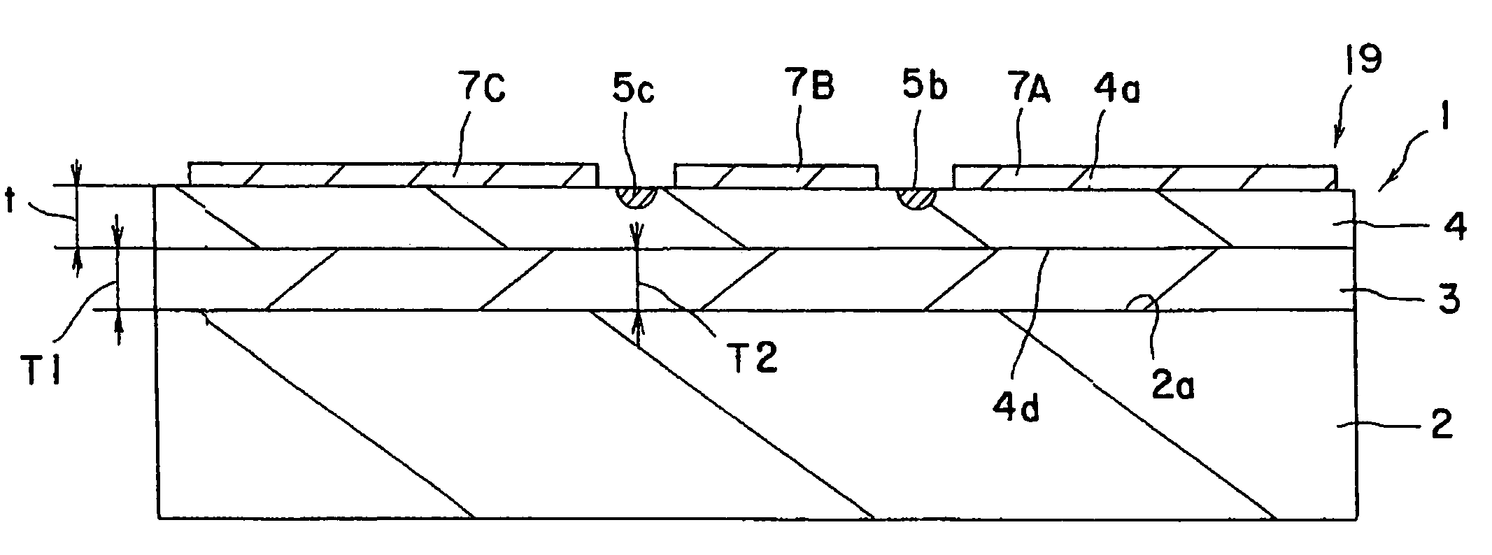
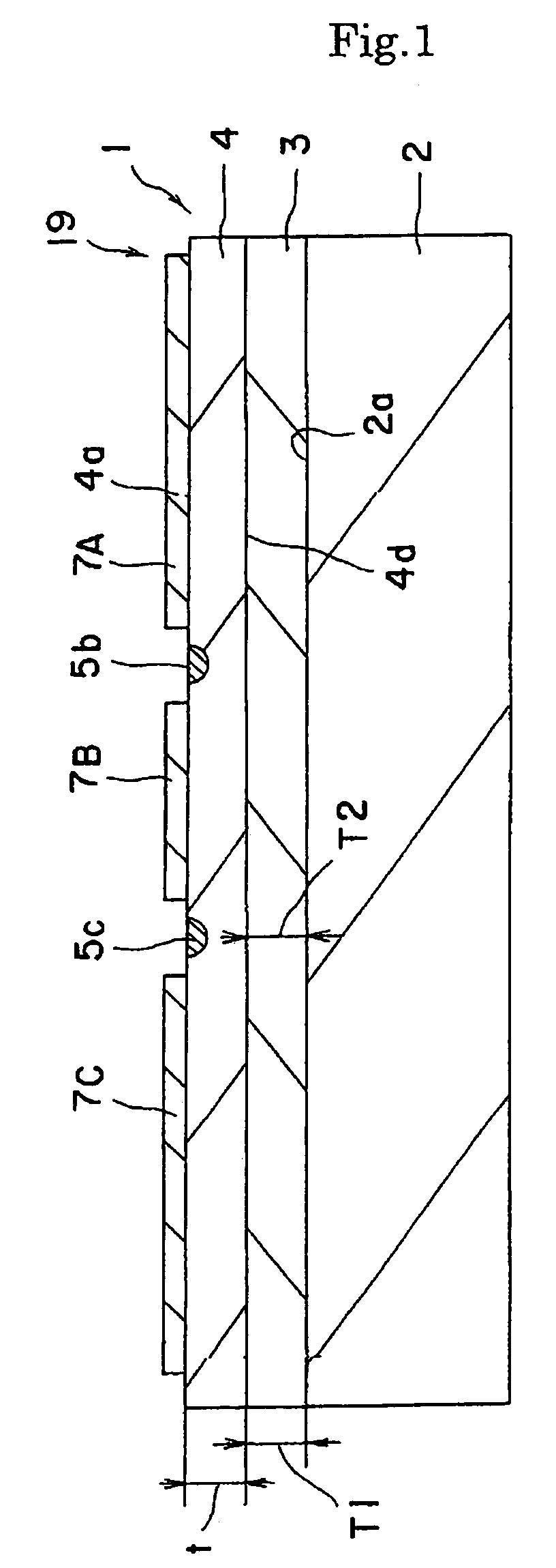
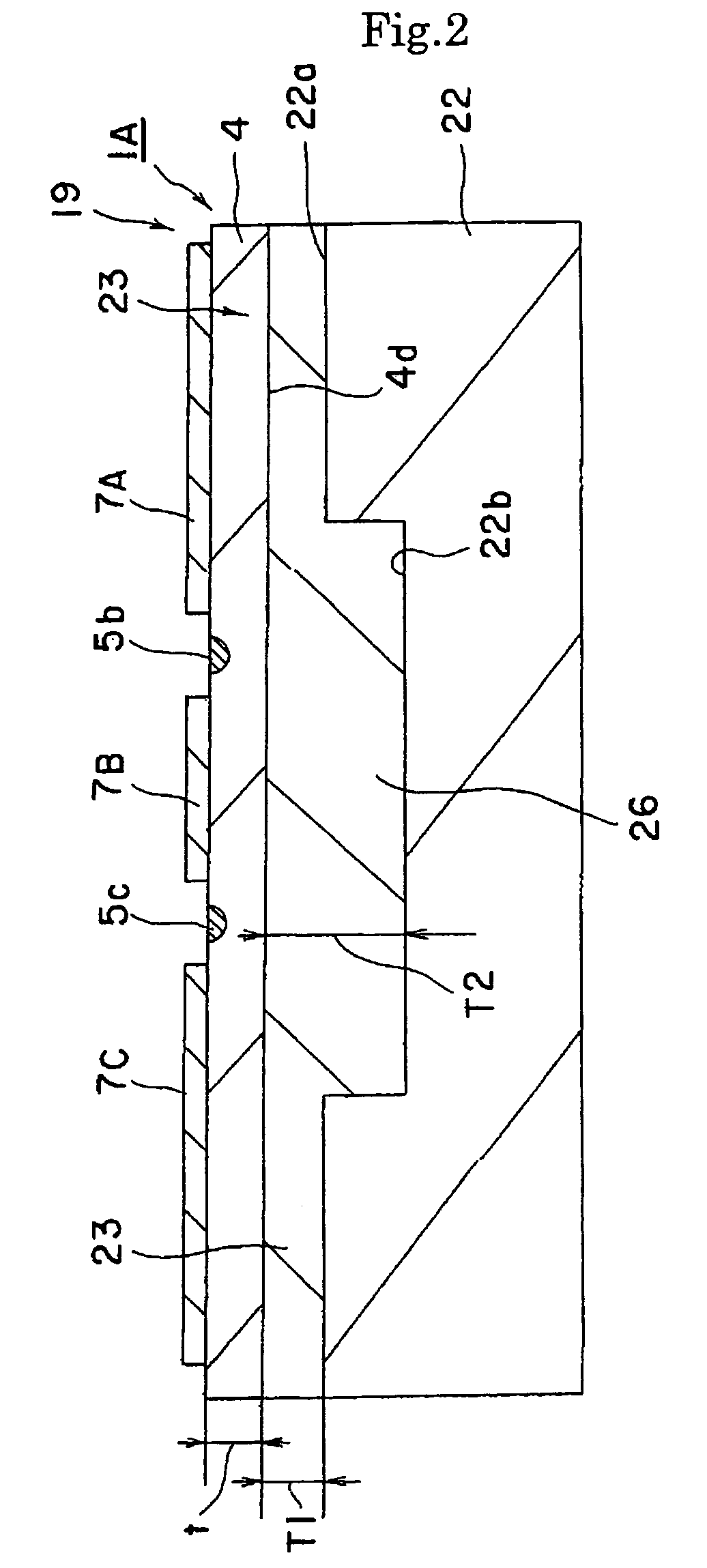
[0075]An optical modulator 1 of FIG. 1 is produced. Specifically, an X-cut 3 inch wafer (made of LiNbOx single crystal) was used as a substrate. An optical waveguide 3 of Mach-Zehnder type was formed in the surface area of the wafer by titanium diffusion with photolithography method. The size of the optical waveguide 3 was, for example, 10 μm at 1 / e2. CPW electrodes were formed by electroplating. The gaps between the central electrode 7B and ground electrodes 7A and 7C are 40 μm, the thickness of the electrode is 28 μm and the length of electrode is 40 μm. A dummy substrate for polishing is adhered to a surface plate for polishing and the substrate for modulator is adhered to the plate with a thermoplastic resin with the electrodes facing downwardly. Further, the thickness of the main body 4 is reduced to 10 μm by lateral grinding and polishing (CMP). The main body 4 is then joined with a supporting body 2 having a shape of a flat plate with an adh...


PUM

PropertyMeasurementUnit
thicknessaaaaaaaaaa
thicknessaaaaaaaaaa
thicknessaaaaaaaaaa

Abstract

An optical waveguide device 1 has an optical waveguide substrate 19, a supporting body 2 for supporting the substrate 19 and a joining layer 3 for joining the substrate 19 and the supporting body 2. The substrate 19 has a flat plate-shaped main body 4 made of an electro-optic material with a thickness of 30 μm or smaller and having first and second main faces 4a and 4b opposing each other, an optical waveguide provided on the side of the first main face 4a of the main body 4, and electrodes 7A to 7C provided on the side of the first main face 4a of the main body 4. The joining layer 3 joins the supporting body 2 at a joining face 4d and the second main face 4d of the main body 4. The joining face 2a of the supporting body 2 is substantially flat. Alternatively, the joining layer 3 has a thickness of 200 μm or lower.

Description

FIELD OF THE INVENTION[0001]The present invention relates to optical waveguide devices and travelling-wave optical modulators utilizing the same.BACKGROUND OF THE INVENTION[0002]It has been strongly demanded to realize a broadband modulation of communication as the progress in the field of so-called multi media. An optical transmission system is thus in use at a frequency of 10 Gb / s or higher, and more high speed modulation is expected. An LN optical modulator has been used as an a device for modulating light by an electrical signal (microwave signal) at 10 Gb / s or higher.[0003]It has been invented a structure for realizing the velocity matching between microwave signal and light wave by forming a thinner portion in an optical waveguide substrate, so that the modulating bandwidth of the optical modulator is made broader. It is described to form a groove at the back side of an optical waveguide substrate in Japanese patent publications 10-82, 921A and 2001-6651A.[0004]Further, in a s...

Claims


Application Information

Patent Timeline
Patent Type & Authority Patents(United States)
IPC IPC(8): G02F1/035G02B6/12G02F1/03G02F1/225
CPCG02F1/0305G02F1/035G02F1/2255G02F1/225G02F1/0123G02F1/0356G02F2203/21G02F2201/503G02F2202/28G02F2202/42
Inventor KONDO, JUNGOKONDO, ATSUOAOKI, KENJIMITOMI, OSAMU
Owner NGK INSULATORS LTD
Why Eureka
Try Eureka