Printed circuit board and producing method for the same

a technology of printed circuit boards and production methods, which is applied in the direction of transfer patterning, circuit inspection/indentification, lithography/patterning, etc., can solve the problems of heavy burden on the circuit board supplier, difficulty in developing circuit boards, and difficulty in forming copper foil patterns, etc., to achieve high visibility, easy to obtain

Inactive Publication Date: 2006-11-16
FUJIFILM CORP +1
View PDF16 Cites 7 Cited by
  • Summary
  • Abstract
  • Description
  • Claims
  • Application Information

AI Technical Summary

Benefits of technology

[0014] The printed circuit board having this kind of the colored patterns possesses high visibility. Although it is possible to produce such a printed circuit board by a conventional method of screen printing and so forth, it is preferable that printing is performed by means of a printer having simplicity of producing. A printing manner of the printer to be used for producing the printed circuit board is not especially limited. However, it is preferable to use an ink-jet printer and a thermal transfer printer, which are versatile and easily obtainable. The printed circuit board having high visibility can be easily produced by loading a conductive ink and a conductive-ink ribbon into the ink-jet printer and the thermal transfer printer.
[0015] According to the present invention, it is possible to grasp the sort of the signal, which is carried thro

Problems solved by technology

In a step for producing the above-mentioned circuit board, it is troublesome and expensive to form a copper-foil pattern and to perform an attachment operation of a base and a cover lay.
Meanwhile, if specification of a new circuit board is changed in the middle of the design thereof, development process of the circuit board is delayed

Method used


Image

  • Printed circuit board and producing method for the same
  • Printed circuit board and producing method for the same
  • Printed circuit board and producing method for the same

Examples


Embodiment Construction

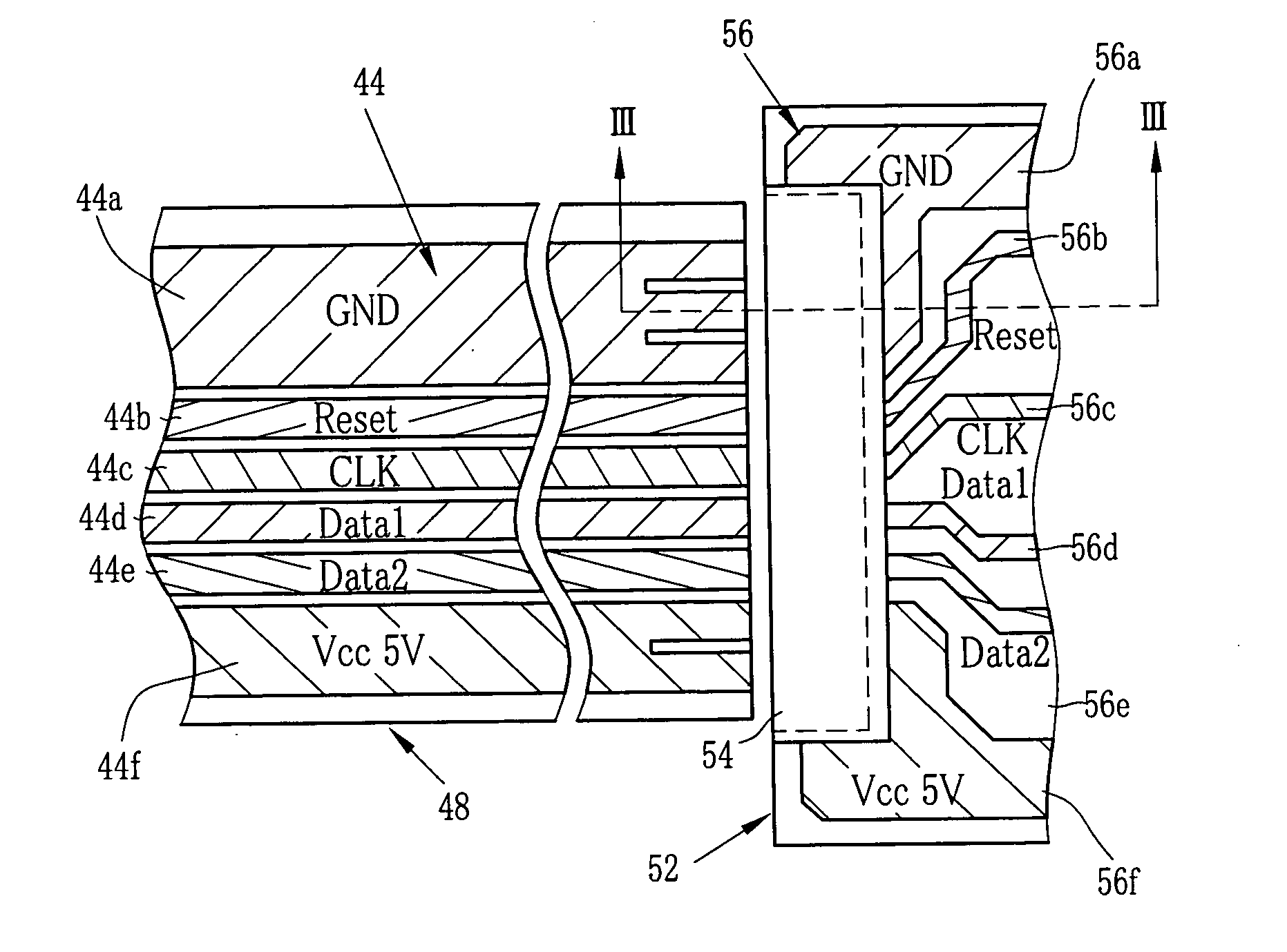
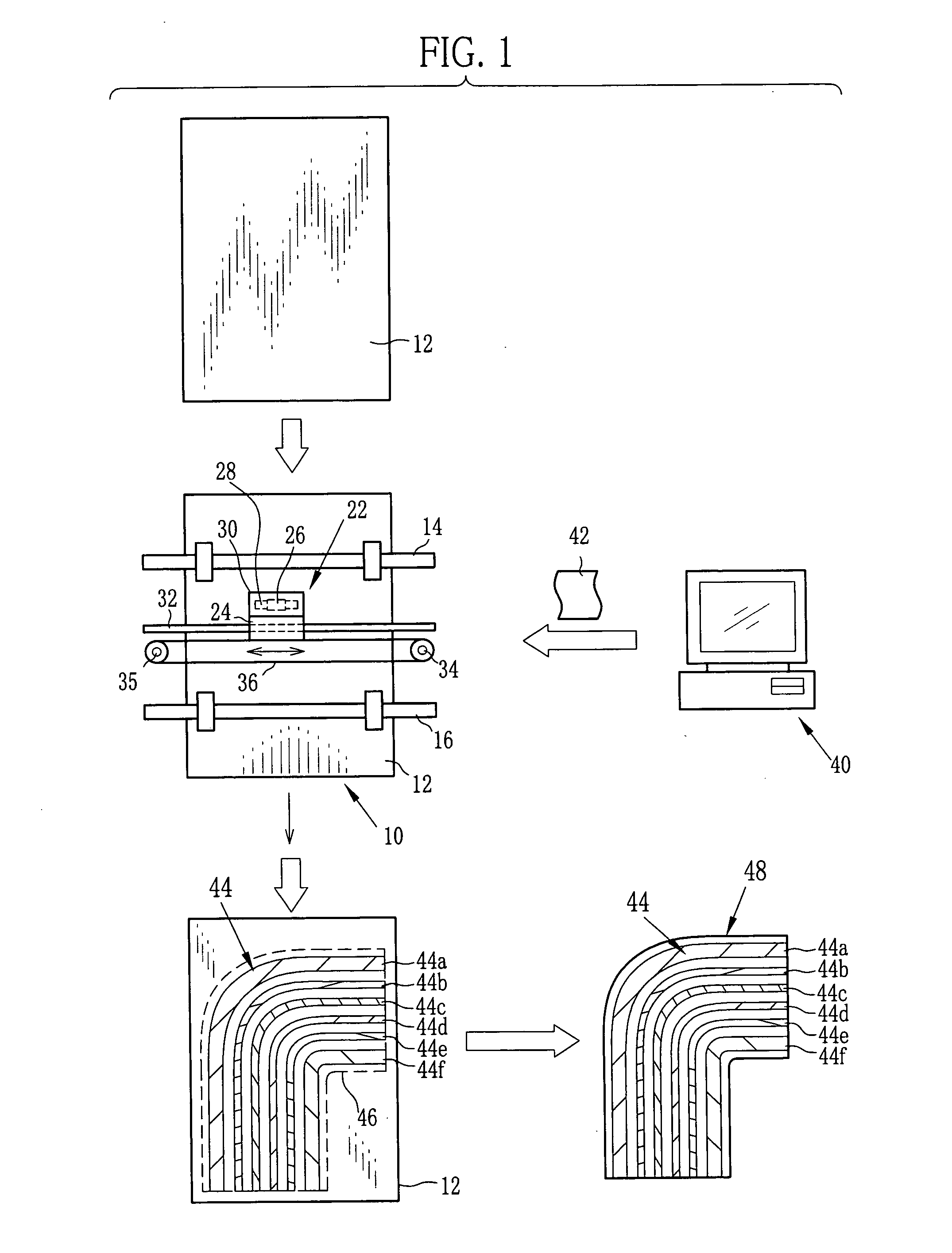
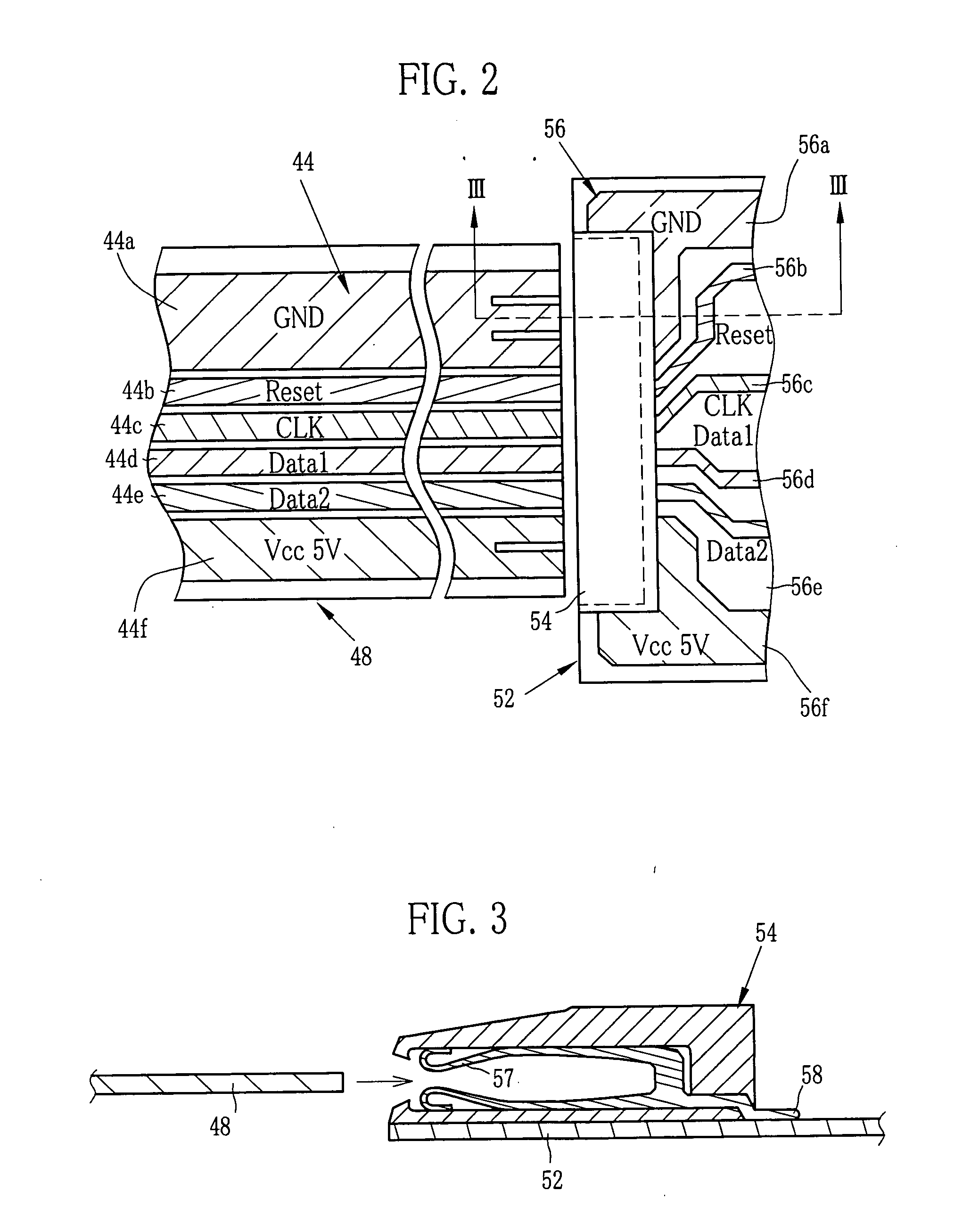
[0021] A first embodiment of the present invention is described below. A flexible substrate 12 is set to a paper feed port of a thermal transfer printer 10 shown in FIG. 1. The flexible substrate 12 is drawn from the paper feed port by a paper roller pair 14 and passes through a carrying roller pair 16. A sensor for detecting an anterior end of the substrate 12 is disposed at a downstream side of the carrying roller pair 16. Upon detecting the anterior end of the flexible substrate 12, a detection signal is sent to a system controller built in the thermal transfer printer 10. In response to receipt of the anterior-end detection signal, the system controller shifts a pinch roller of the carrying roller pair 16 to nip the flexible substrate 12.

[0022] The paper roller pair 14 and the carrying roller pair 16 are driven by a motor. While printing is performed, the carrying roller pair 16 is rotated in a forward direction so as to intermittently carry the flexible substrate 12 in a feedi...


PUM

PropertyMeasurementUnit
Electrical conductivityaaaaaaaaaa
Coloraaaaaaaaaa
Densityaaaaaaaaaa

Abstract

A thermal transfer printer is used for printing colored patterns on a flexible material. A conductive-color-ink ribbon contains inks of cyan, magenta and yellow in which conductive powders are added. The colored pattern formed by using this ink ribbon has conductivity. The colored patterns are separated by color every pattern through which an identical circuit signal is carried. As to the color-coded patterns, it is possible to distinguish the pattern through which another circuit signal is carried. An FPC comprising the color-coded patterns has high pattern-visibility so that it is possible to prevent improper connection or the like from occurring.

Description

FIELD OF THE INVENTION [0001] The present invention relates to a printed circuit board having a colored pattern formed by a color printer, and further relates to a producing method for the printed circuit board. BACKGROUND OF THE INVENTION [0002] A conductor for forming an electronic circuit is formed on a printed circuit board. The conductor is composed of pads, lands and wiring patterns. A semiconductor device package of an IC and so forth is fixed to the pads. Moreover, electronic parts of a resistor, a capacitor and so forth are also fixed to the pads. The land is a connection area for performing wiring on both surfaces of a substrate and for performing wiring in each layer of a multi-layer substrate. The wiring pattern connects a lead of the respective parts, the pads and the lands. [0003] Regarding the printed circuit board (hereinafter referred to as PCB) having the conductor, it is required to satisfy various conditions concerning electrical insulation, heat resistance, mois...

Claims


Application Information

Patent Timeline
IPC IPC(8): H05K1/14
CPCH05K1/0269H05K1/095H05K3/046H05K3/125H05K2203/161H05K2201/09936H05K2203/013H05K2203/0528H05K2201/0391
Inventor MUROKI, SEISUKE
Owner FUJIFILM CORP
Why Eureka
Try Eureka