Component-embedded printed wiring board and method of manufacturing the same

Inactive Publication Date: 2006-11-23
PANASONIC CORP
View PDF2 Cites 12 Cited by
  • Summary
  • Abstract
  • Description
  • Claims
  • Application Information

AI Technical Summary

Problems solved by technology

The conventional PWB, however, has the following problem if components 3 are densely mounted.
Thickness T1 of substrate 2c is 75 μm, so that width W2 of frame 10a becomes smaller than thickness T1 of substrate 2c, and it becomes physically difficult to manufacture this

Method used


Image

  • Component-embedded printed wiring board and method of manufacturing the same
  • Component-embedded printed wiring board and method of manufacturing the same
  • Component-embedded printed wiring board and method of manufacturing the same

Examples


embodiment 1

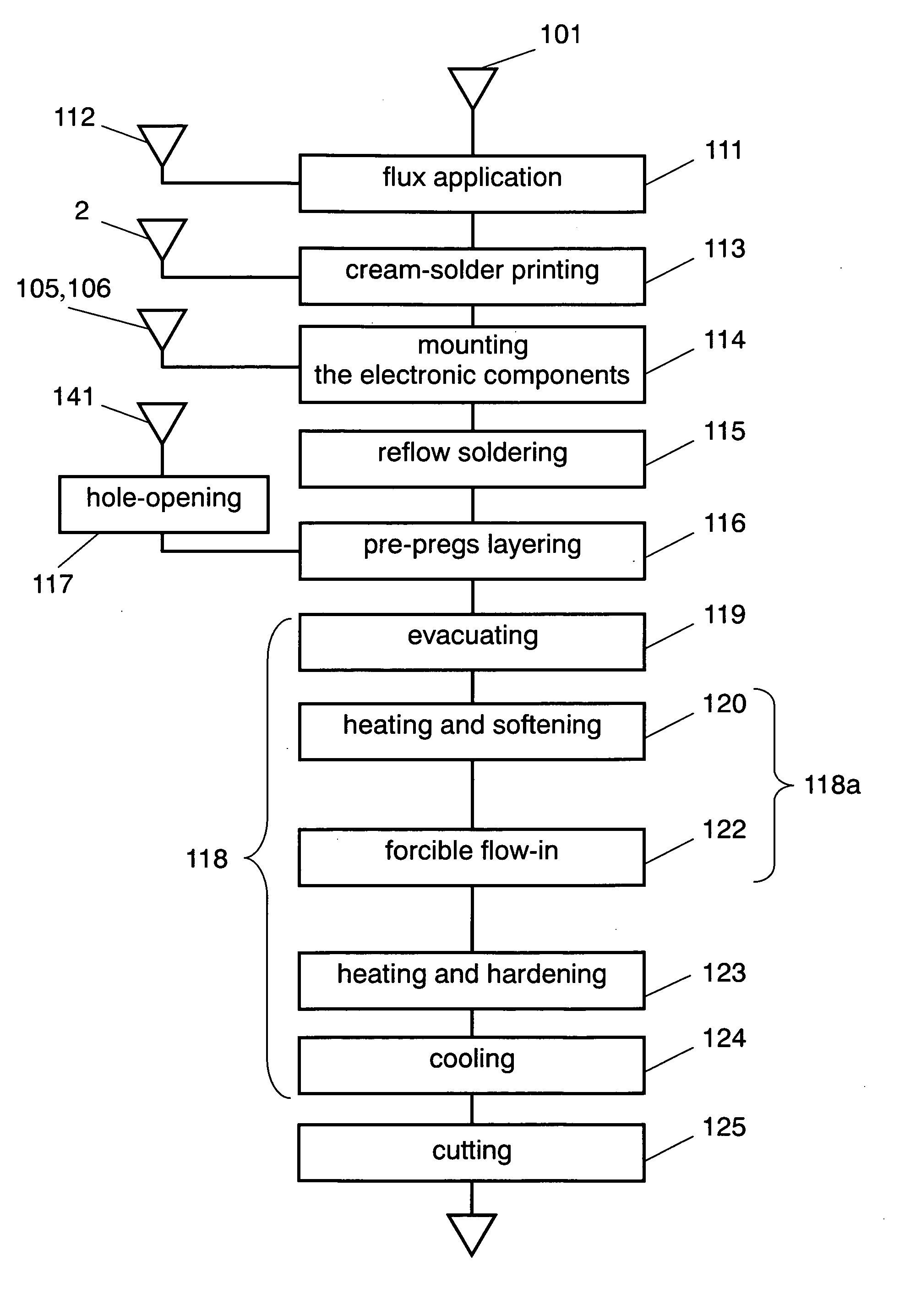
[0045] The first exemplary embodiment of the present invention is demonstrated hereinafter with reference to FIG. 1-FIG. 12. FIG. 1 shows a sectional view of a component-embedded printed wiring board (PWB) in accordance with the first embodiment of the present invention. FIG. 2 shows a flowchart illustrating the steps of manufacturing the component-embedded PWB. FIG. 3-FIG. 12 detail respective manufacturing steps of the component-embedded PWB in accordance with the first embodiment. In these drawings, similar elements to those of the prior art have the same reference marks, and the descriptions thereof are simplified.

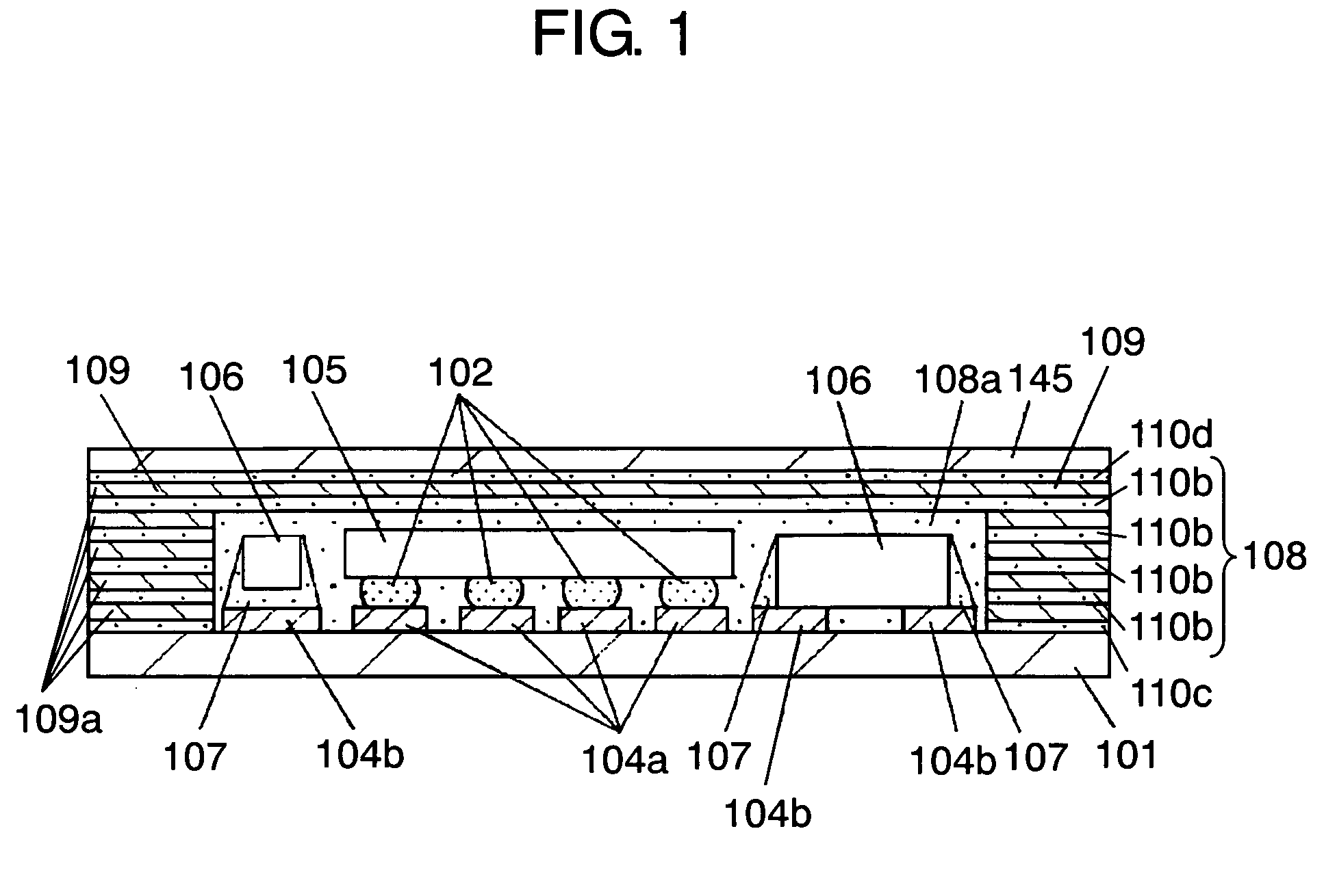
[0046] The construction of the component-embedded PWB in accordance with the first embodiment is described with reference to FIG. 1. Circuit board 101 shown in FIG. 1 is formed of thermosetting resin in multi-layer structure. Board 101 has inner via-holes (not shown) which connect respective top faces to respective undersides of each layer. The respective top faces ha...

embodiment 2

[0130] The second embodiment of the present invention is demonstrated hereinafter with reference to FIGS. 17-20. FIG. 17 shows a flowchart illustrating the steps of manufacturing a component-embedded printed wiring board (PWB) in accordance with this second embodiment. In FIGS. 17-20, similar elements to those shown in FIGS. 1-12 have the same reference marks, and the descriptions thereof are simplified here. In the first embodiment previously discussed, six sheets of pre-pregs 141 are layered on circuit board 101; however, in this embodiment, only one sheet of pre-preg having a thickness of approx. 1 mm is layered on circuit board 101. The respective steps are detailed hereinafter following the sequence of the steps shown in FIG. 17.

[0131] In this second embodiment, as the first embodiment demonstrates, semiconductor element 105 and resistor 106 are mounted on circuit board 101, and they undergo the soldering in reflow soldering step 115. After step 115, hanging step 300 is prepar...

embodiment 3

[0152] In the third embodiment, another instance of the decompressing and layering device described in the second embodiment is demonstrated, and this another device can replace the one used in the second embodiment. The respective manufacturing steps in the third embodiment remain unchanged from those in the second embodiment. Thus only this replaceable decompressing and layering device is described hereinafter.

[0153]FIGS. 21 and 22 show sectional views of the decompressing and layering device used in the decompressing and layering step in accordance with the third embodiment. FIG. 23 shows a sectional view of the component-embedded PWB in the forcible flow-in step of the third embodiment. In these drawings, elements similar to those used in FIG. 1-FIG. 20 sometimes have the same reference marks, and in such cases the descriptions thereof are simplified.

[0154] In FIG. 21, platens 151, 152 and expandable wall 153 form airtight container 154. Circuit board 101, on which semiconduct...


PUM

PropertyMeasurementUnit
Temperatureaaaaaaaaaa
Pressureaaaaaaaaaa
Flow rateaaaaaaaaaa

Abstract

A component-embedded printed wiring board (PWB) is disclosed. This PWB includes (a) a fluid-resin embedding section formed at place corresponding to electronic components such that the embedding section covers the electronic components, (b) a resin flow-speed accelerator placed in parallel with a top face of a circuit board and surrounding the embedding section, and (c) bonding resin placed at least between the accelerator and the circuit board. The fluid resin embedding section is filled up with the same resin as the bonding resin. This structure allows the accelerator to compress the resin with a pressure applied to the PWB, so that the resin tends to flow along the circuit board. As a result, the fluid-resin embedding section is thoroughly filled up with the resin without leaving any airs, and the reliable PWB is thus obtainable.

Description

FIELD OF THE INVENTION [0001] The present invention relates to a component-embedded printed wiring board which includes electronic components built therein, and a method of manufacturing the same printed wiring board. BACKGROUND OF THE INVENTION [0002] A conventional component-embedded printed wiring board (PWB) is described hereinafter. FIG. 24 shows a structure of the conventional PWB which includes electronic components built therein. As shown in FIG. 24, the conventional PWB comprises plate 1 made of metallic material, and substrates 2a-2e formed of thermoplastic resin and layered over metallic plate 1. [0003] Holes 4 are opened through substrates 2c and 2d for embedding electronic component 3. Patterns 5 are provided on substrates 2a-2e, and via-holes 7 opened through substrates 2a-2e are filled with conductive paste 6. Electrodes 8 placed at both sides of component 3 are conductive to paste 6. [0004] Conductive paste 6 is made by mixing tin grains with silver grains. Between c...

Claims


Application Information

Patent Timeline
IPC IPC(8): H05K1/00H05K3/00
CPCH01L2224/16225H05K1/186H05K3/284Y10T29/4913Y10T29/49124Y10T29/49144Y10T29/49146H05K3/4652H01L2924/00014H01L2924/00011H01L2924/19105H01L2924/3511H01L2224/0401
Inventor HONJO, KAZUHIKOMORI, TOSHIHIKOKAWAMOTO, EIJIKIMURA, JUNICHIKITAGAWA, MOTOYOSHI
Owner PANASONIC CORP
Why Eureka
Try Eureka