Single-transistor-control low-dropout regulator

a regulator and single-transistor technology, applied in the direction of electric variable regulation, process and machine control, instruments, etc., can solve the problems of ldo regulator stability, limiting the choice of output capacitance combinations, and difficult optimization between stability and transient respons

Active Publication Date: 2006-11-23
THE HONG KONG UNIV OF SCI & TECH
View PDF3 Cites 18 Cited by
  • Summary
  • Abstract
  • Description
  • Claims
  • Application Information

AI Technical Summary

Benefits of technology

[0023] The DC-biasing circuit may provide a DC voltage difference between the control electrode of the pass transistor and the output electrode of the control transistor whereby the control transistor operates in the saturation region.
[0024] The DC-biasing circuit preferably comprises a second biasing-current source and a resistive element. The second biasing-current source may be connected between ground and the control electrode of the pass transistor, the resistive element is interposed between the control electrode of the pass transistor and the output electrode of the control transistor, and the second biasing-current source provides biasing current to the resistive element, which produces a DC voltage difference between the control electrode of said pass transistor and the output electrode of the control transistor. The resistive element may be a resistor connected between the control electrode of the pass transistor and the output electrode of the control transistor, or alternatively may be a P-channel Metal-Oxide-Silicon Field-Effect-Transistor (PMOSFET) or a PNP bipolar junction transistor.
[0025] Preferably the source / emitter electrode of the PMOSFET / PNP bipolar junction transistor is coupled to the output electrode of the control transistor, the drain / collector electrode of the PMOSFET / PNP bipolar junction transistor is connected to the control electrode of the pass transistor, and the voltage applied on the gate / base electrode of the PMOSFET / PNP bipolar junction transistor is used to control the source-to-drain / emitter-to-collector resistance whereby a suitable DC voltage difference is provided between the control electrode of the pass transistor and the output electrode of the control transistor.
[0026] The reference mirror circuit may comprise a diode-connected transistor, a current mirror, a transconductance Gm-cell and a third biasing-current source. Preferably, within tolerances the diode-connected transistor has the same dimensions and consumes the same current as the control transistor. Preferably within tolerances the voltage across the low-impedance electrode and the control electrode of both the diode-connected transistor and the control transistor are the same whereby the output voltage of said regulator equals the voltage applied to the low-impedance electrode of the diode-connected transistor. The diode-connected transistor may be a NMOSFET or a NPN bipolar junction transistor. Both the drain / collector electrode and the gate / base electrode of the diode-connected transistor and the third biasing-current source may be connected to form the output terminal of the reference mirror circuit and thereby generating a control voltage biased to the control electrode of the control transistor.
[0027] In one embodiment of the invention the current mirror comprises two NMOSFETs or NPN bipolar junction transistors. In this embodiment the source / emitter electrodes of both NMOSFETs / NPN bipolar junction transistors are coupled to ground, and one of the NMOSFETs / NPN bipolar junction transistors is diode-connected to sense the output current of Gm-cell, whereby by connecting the gate / base electrodes of both said NMOSFETs / NPN bipolar junction transistors the sensed output current of Gm-cell is mirrored to the low-impedance electrode of the diode-connected transistor.
[0028] Preferably both the current mirror and the Gm-cell mirror the supply- and temperature-independence reference voltage to the low-impedance electrode of the diode-connected transistor with current-driving capability. Preferably the reference mirror circuit accepts a supply- and temperature-independent reference voltage and mirrors this reference voltage to the output terminal of the regulator by generating a control voltage biased to the control electrode of the control transistor.

Problems solved by technology

To provide such frequency compensation dominant-pole compensation and pole-zero cancellation are commonly used in the art, but these limit the choices of combinations of the output capacitance (COUT) and its equivalent-series-resistance (RESR) for LDO regulator stability.
Furthermore, since the loop bandwidth of a conventional LDO is degraded by dominant-pole compensation, optimization between stability and transient response is difficult to achieve.

Method used


Image

  • Single-transistor-control low-dropout regulator
  • Single-transistor-control low-dropout regulator
  • Single-transistor-control low-dropout regulator

Examples


Embodiment Construction

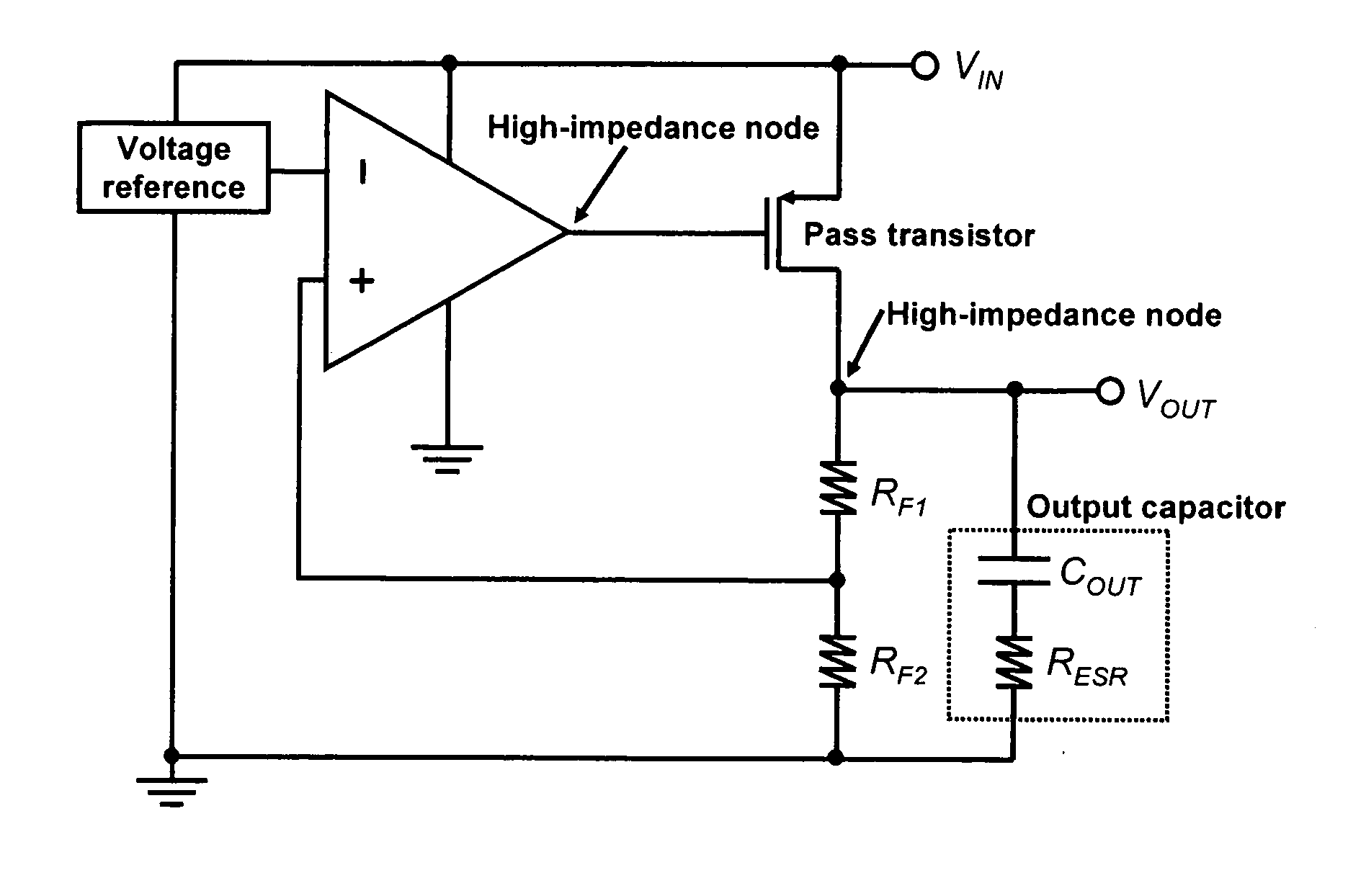
[0035] This invention provides a LDO regulator with improved transient response and stability based on the concept of providing ultra-low resistance, which can be dynamically changed according to VOUT, at the output of the LDO regulator, even though the pass transistor itself has high output resistance.

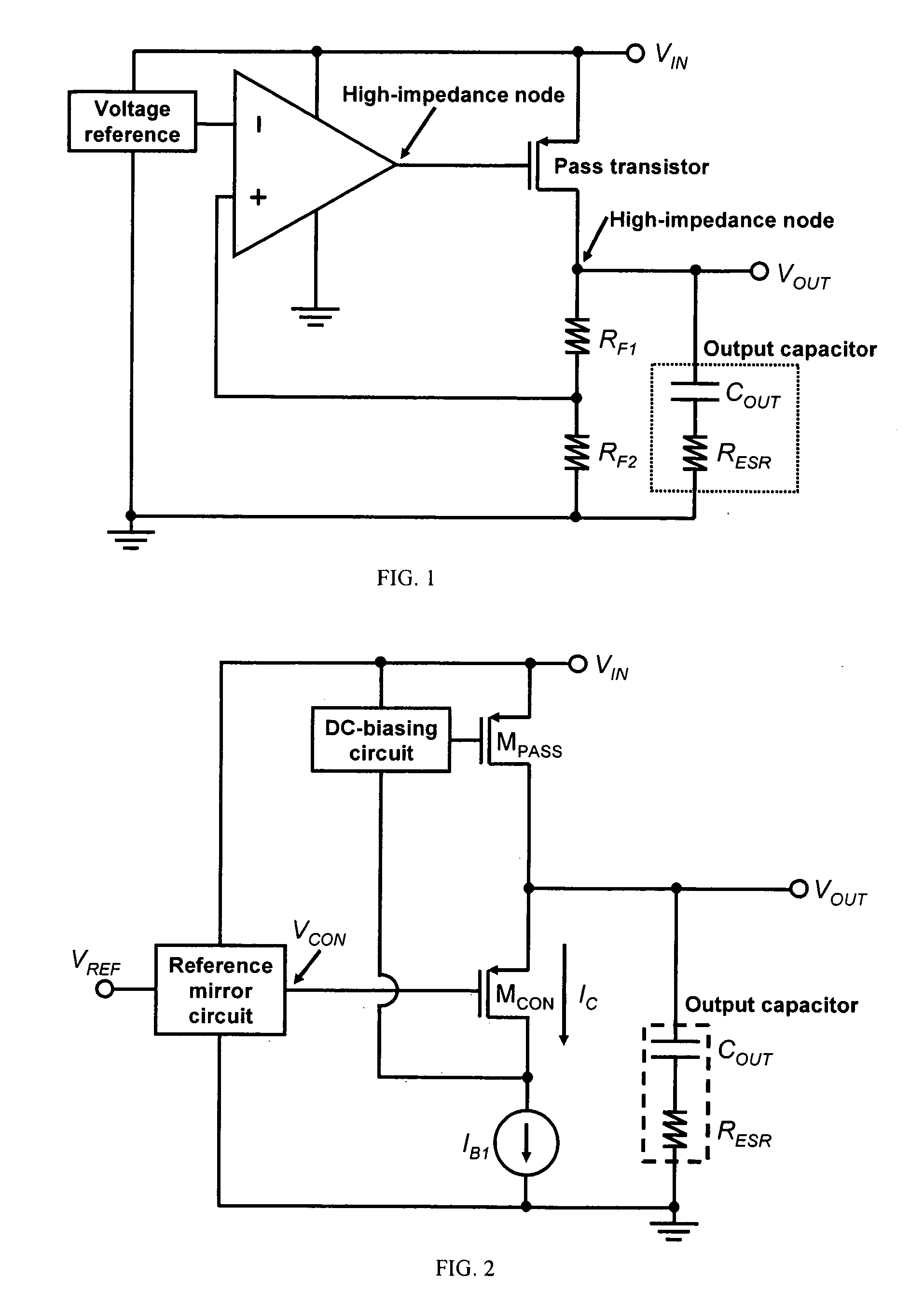
[0036]FIG. 2 shows the basic structure of an embodiment of the LDO regulator in accordance with this invention, including a pass transistor MPASS, a control transistor MCON, a DC-biasing circuit, a reference mirror circuit, a first biasing-current source IB1 and an optional output capacitor. MPASS is interposed between VIN and VOUT. The gate electrode of MPASS is coupled to one end of the DC-biasing circuit. The source electrode of MCON is connected to VOUT. The gate electrode of MCON is biased by a control voltage VCON, which is generated by the reference mirror circuit. The drain electrode of MCON is coupled to one end of the current source and one end of the DC-biasing circuit. An...


PUM


Abstract

A low-dropout regulator with a single-transistor-control providing improved transient response and stability is disclosed. The single-transistor-control provides a dynamic resistance at the output of the regulator for minimizing undershoot and overshoot, and hence improves transient response. Since the single-control transistor reduces the output resistance of the regulator, the output pole is pushed to a sufficiently high frequency without affecting stability. Therefore, the limited choice of combinations of the output capacitance and its equivalent-series-resistance is substantially relaxed.

Description

CROSS-REFERENCE TO RELATED APPLICATION [0001] This application claims the benefits of U.S. Provisional Application No. 60 / 658,752 filed on Mar. 7, 2005, which is hereby incorporated herein by reference in its entirety.FIELD OF THE INVENTION [0002] This invention relates to a low-dropout regulator, and in particular, to a low-dropout regulator that has improved transient response and stability. BACKGROUND OF THE INVENTION [0003] A low-dropout (LDO) regulator accepts an unregulated input voltage (VIN) and provides a regulated output voltage (VOUT) that is nearly independent of output current (e.g. a load current). A PMOS pass transistor is used to minimize the voltage difference between the input and output of a LDO regulator, and hence increases power conversion efficiency. [0004]FIG. 1 shows the schematic of a typical LDO regulator according to the art, which consists of a pass transistor, an error amplifier, a reference voltage, a feedback resistor network and an optional output ca...

Claims


Application Information

Patent Timeline
Patent Type & Authority Applications(United States)
IPC IPC(8): G05F3/20
CPCG05F1/575
Inventor MAN, TSZ YINLEUNG, CHI YATLEUNG, KA NANGMOK, PHILIP KWOK TAICHAN, JOHN MAN SUN
Owner THE HONG KONG UNIV OF SCI & TECH
Why Eureka
Try Eureka