Apparatus and method for defect inspection

a technology of defect inspection and apparatus, applied in the field of defect inspection apparatus and method, can solve the problems of limiting the enhancement of resolving power, unable to improve the spatial frequency itself for the resolution limit, and the defect to be inspected is becoming more and more microscopic. , to achieve the effect of high sensitivity

Inactive Publication Date: 2006-11-23
HITACHI HIGH-TECH CORP
View PDF6 Cites 44 Cited by
  • Summary
  • Abstract
  • Description
  • Claims
  • Application Information

AI Technical Summary

Benefits of technology

[0012] According to the present invention, it becomes possible to illuminate an inspection-target object at only an incident angle at which the gray-scale contrast of the microscopic defects will be emphasized more sharply. This characteristic allows the gray-scale contrast of the microscopic defects to be emphasized more sharply than the gray-scale contrast of the microscopic patterns, thereby making it possible to detect the microscopic defects with a high sensitivity.

Problems solved by technology

In recent years, however, the defects to be inspected have become more and more microscopic in accompaniment with the enhancement in the integration scale of semiconductor devices.
Namely, there exists a limit to the enhancement in the resolving power which is based on the shorter-wavelength implementation.
Accordingly, this method cannot improve the spatial frequency itself for the resolution limit.
Consequently, there has existed a problem that it is impossible to enhance the detection sensitivity for the microscopic defects further than that.

Method used


Image

  • Apparatus and method for defect inspection
  • Apparatus and method for defect inspection
  • Apparatus and method for defect inspection

Examples


embodiment 1

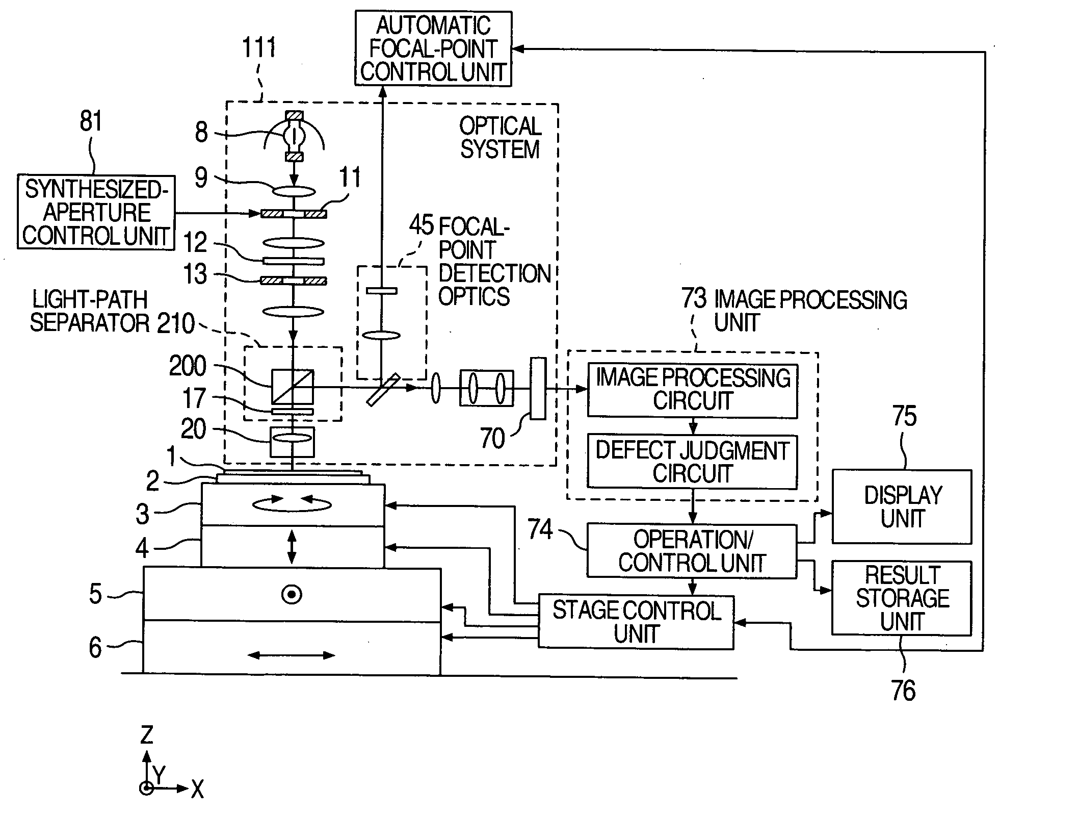
[0029]FIG. 1 illustrates an embodiment of the optical defect inspection apparatus using a microscopic-defect detection method according to the present invention. A semiconductor wafer 1, which is an inspection-target object, adheres to a wafer chuck 2 through vacuum absorption. This wafer chuck 2 is mounted on a O stage 3, a Z stage 4, a Y stage 5, and an X stage 6. An optics 111 located above the semiconductor wafer 1 photographs an optical image of the semiconductor wafer 1 in order to perform defect inspection of patterns formed on the semiconductor wafer 1. The optics 111 mainly includes an illumination optics, an image-formation optics for creating and imaging the image of the semiconductor wafer 1, and a focal-point detection optics 45. A light-source 8 located in the illumination optics is an incoherent light-source, which is, e.g., a xenon lamp.

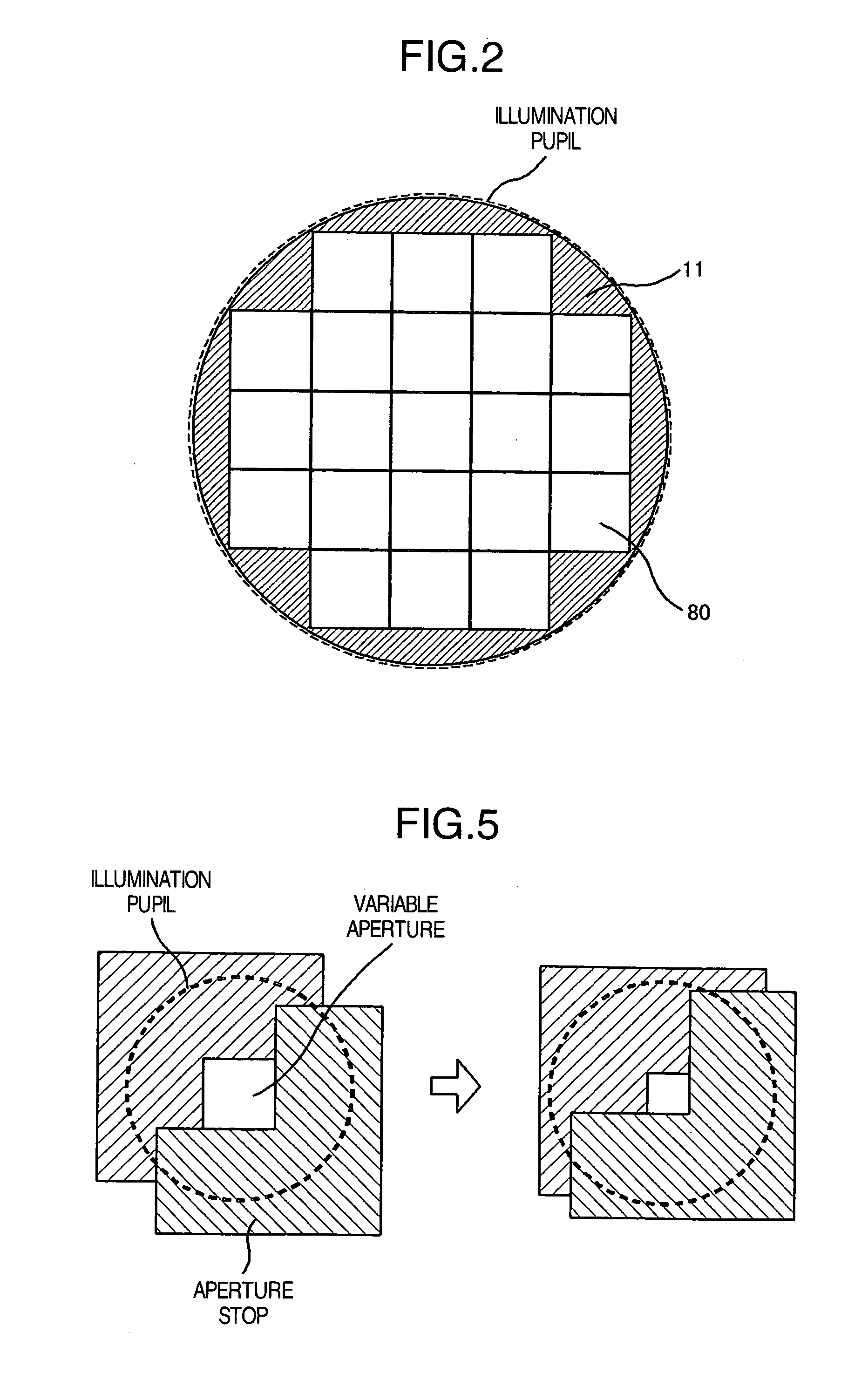
[0030] Light emitted from the light-source 8 passes through an aperture portion of an aperture stop 11 located on an illumination p...

embodiment 2

[0046] Next, FIG. 6 illustrates another embodiment of the optical defect inspection apparatus using the microscopic-defect detection method according to the present invention. Except the configurations of the light-source and the illumination optics, the other configurations are in common with the first embodiment illustrated in FIG. 1. Accordingly, the explanation about the other configurations will be omitted. In the present embodiment, the light-source 8 located in the illumination optics is a laser light-source.

[0047] Light emitted from the light-source 8 is shaped by a beam shaper 85 in its beam cross-section configuration. Even after the shaping, cross-section area of the laser beam is smaller than the illumination pupil. This laser beam performs incidence into a light-flux fluctuation system 86. Based on an instruction from a deflection control unit 87, the light-flux fluctuation system 86 is capable of deflecting the laser beam so that the laser beam will pass through an ar...


PUM

PropertyMeasurementUnit
wavelengthaaaaaaaaaa
refractive indexaaaaaaaaaa
defect inspectionaaaaaaaaaa

Abstract

In the conventional methods for enhancing defect detection sensitivity by improving the resolving power, if a microscopic pattern, which is a high spatial-frequency structure as is the case with a microscopic defect, has become the brightest portion, the gray-scale contrast of the microscopic defect will be enhanced. At the same time, however, the gray-scale contrast of the microscopic pattern will also be enhanced simultaneously. Consequently, there has existed a problem that it is impossible to enhance the microscopic-defect detection sensitivity further than that. In the present invention, an aperture stop which is divided into a plurality of small apertures is located on an illumination pupil plane. Then, light-shield/light-transmission for each small aperture is controlled independently of each other. This control allows an inspection-target object to be illuminated at only an incident angle at which the gray-scale contrast of the microscopic defect will be emphasized more sharply.

Description

BACKGROUND OF THE INVENTION [0001] 1. Field of the Invention [0002] The present invention relates to a defect inspection apparatus and method for inspecting defects existing on an inspection-target object. More particularly, it relates to a defect inspection apparatus and method used for observing and inspecting defects and foreign substances on microscopic patterns in fabrication lines such as semiconductor fabrication steps and flat-panel display manufacturing steps. [0003] 2. Description of the Related Art [0004] In the fabrication lines such as semiconductor fabrication steps and flat-panel display manufacturing steps, the observation and inspection of the defects and foreign substances on microscopic patterns are performed using optical microscopes. From the viewpoint of illumination schemes, the microscope optics used for the defect inspection like this are classified into two types, i.e., bright-field illumination scheme and dark-field illumination scheme. Here, the bright-fi...

Claims


Application Information

Patent Timeline
Patent Type & Authority Applications(United States)
IPC IPC(8): G01N21/88
CPCG01N21/956G01N21/8806
Inventor MATSUI, SHIGERUITO, MASAAKI
Owner HITACHI HIGH-TECH CORP
Why Eureka
Try Eureka