Supercritical fluid-assisted direct write for printing integrated circuits

a technology of integrated circuits and supercritical fluids, applied in the direction of printing, printing press parts, basic electric elements, etc., can solve the problems of increasing the drawback of traditional photolithography optical aligners, the most time-consuming and laborious step, and the most expensive chemicals and aligners/steppers. achieve the effect of high resolution, high resolution and high resolution

Inactive Publication Date: 2006-11-30
MICRON TECH INC
View PDF5 Cites 42 Cited by
  • Summary
  • Abstract
  • Description
  • Claims
  • Application Information

AI Technical Summary

Benefits of technology

[0005] The present invention provides a method for printing high resolution patterns provided on a surface of a substrate. The high resolution patterns have dimensions less than 0.1 micron and are formed by a direct writing method employing a supercritical fluid comprising nanometer-sized particles, which may be optionally electrically charged.
[0006] The invention also provides a system for delivering a functional material comprising nanometer-sized particles that are dissolved or dispersed in a supercritical fluid, to produce high resolution patterns with dimensions less than 0.1 micron. The system for producing high resolution patterns includes a print head for delivering a functional material comprising nanometer-sized particles that are dissolved or dispersed in a supercritical fluid and then directing the functional material onto the surface of a substrate. A controlled environment exposes the substrate to receive the functional material as a patterned deposition on the substrate. Optionally, the system may include ...

Problems solved by technology

Although conventional photolithography is widely employed in the formation of patterns on a substrate, photolithography not only requires expensive chemicals and aligners/steppers, but also is typically the most time consuming and labor intensive step.
Additionally, traditional photolithography optical aligners require very flat substrates due to the small depth of focus.
Thi...

Method used


Image

  • Supercritical fluid-assisted direct write for printing integrated circuits
  • Supercritical fluid-assisted direct write for printing integrated circuits
  • Supercritical fluid-assisted direct write for printing integrated circuits

Examples


Embodiment Construction

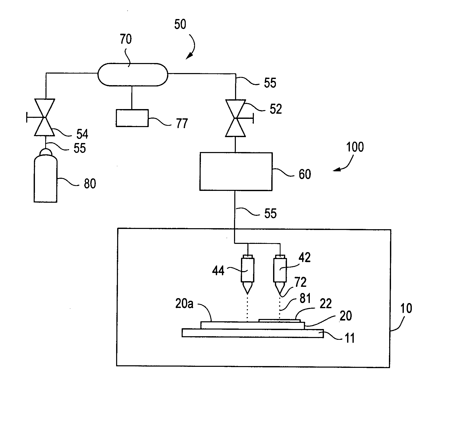
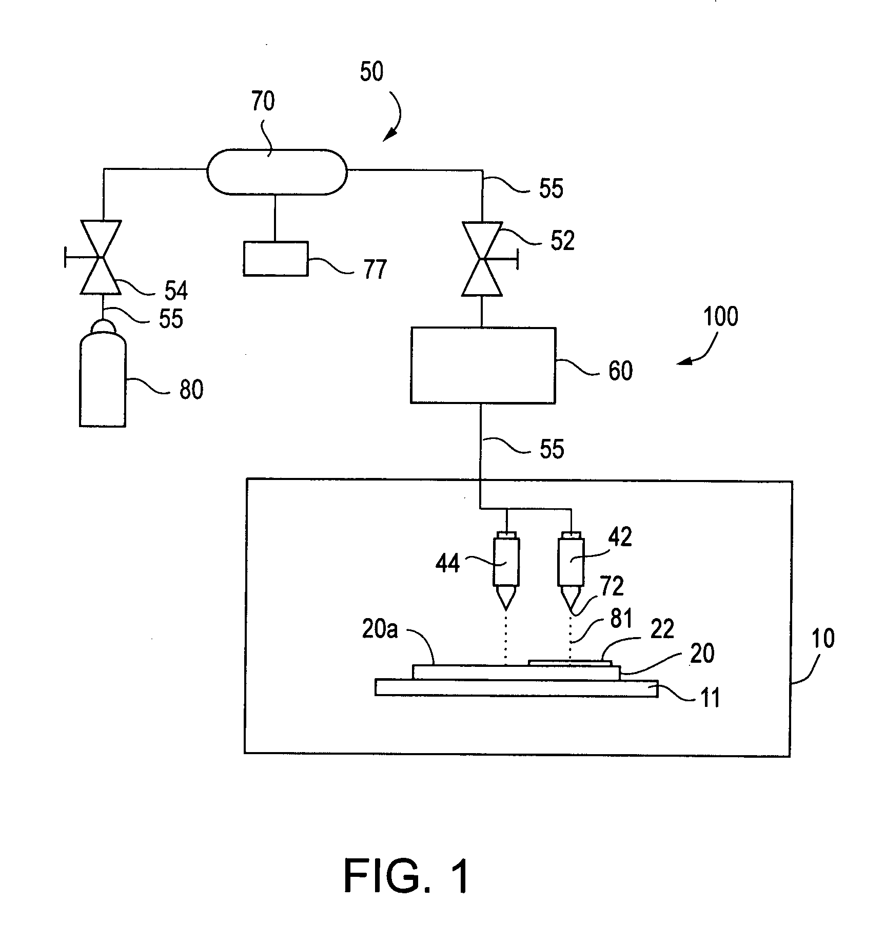
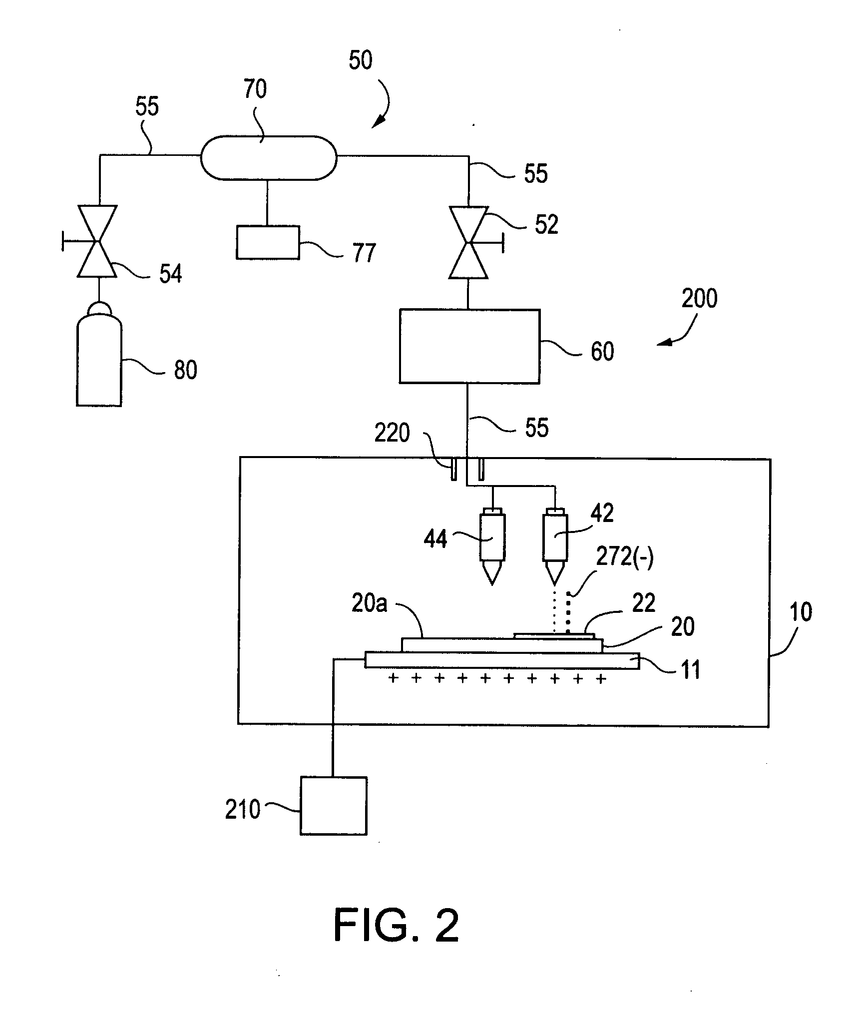
[0012] In the following detailed description, reference is made to the accompanying drawings which form a part hereof, and in which is shown by way of illustration specific embodiments in which the invention may be practiced. These embodiments are described in sufficient detail to enable those skilled in the art to practice the invention, and it is to be understood that other embodiments may be utilized, and that structural, logical and electrical changes may be made without departing from the spirit and scope of the present invention.

[0013] The term “supercritical fluid” relates to materials that are at a temperature and pressure which allows them to be at, above, or slightly below their critical point (the critical point is defined by a critical temperature and a critical pressure). The critical temperature and critical pressure typically define a thermodynamic state in which a fluid or a material becomes supercritical and exhibits gas-like and liquid-like properties. Materials t...


PUM


Abstract

High resolution patterns provided on a surface of a semiconductor substrate and methods of direct printing of such high resolution patterns are disclosed. The high resolution patterns may have dimensions less than 0.1 micron and are formed by a direct writing method employing a supercritical fluid comprising nanometer-sized particles, which may be optionally electrically charged.

Description

FIELD OF THE INVENTION [0001] The invention relates to a method for direct writing integrated circuit (IC) patterns using printing techniques. BACKGROUND OF THE INVENTION [0002] Semiconductors and other electronic components need to be interconnected with each other to form circuits. As semiconductors continue to improve in performance, cost, reliability and miniaturization, there is an intensive need in the electronics industry to package and interconnect these semiconductors without limiting system performance. One approach in patterning metal lines on a substrate is the well-known photolithography technique. Although conventional photolithography is widely employed in the formation of patterns on a substrate, photolithography not only requires expensive chemicals and aligners / steppers, but also is typically the most time consuming and labor intensive step. Additionally, traditional photolithography optical aligners require very flat substrates due to the small depth of focus. Thi...

Claims


Application Information

Patent Timeline
IPC IPC(8): B41F5/18
CPCH01L21/288H01L2924/12044H01L23/5328H01L21/76838H01L2924/0002H01L2924/00B41F33/00
Inventor SANDHU, GURTEJBASCERI, CEM
Owner MICRON TECH INC
Why Eureka
Try Eureka