Semiconductor photodetector and photodetecting device

a technology of photodetector and semiconductor, applied in semiconductor devices, solid-state devices, electrical devices, etc., can solve the problems of inability to maintain high-speed response characteristics, low photodetection sensitivity, and inability to spread the depletion layer easily, and achieve high-speed response characteristics.

Inactive Publication Date: 2006-11-30
HAMAMATSU PHOTONICS KK
View PDF2 Cites 0 Cited by
  • Summary
  • Abstract
  • Description
  • Claims
  • Application Information

AI Technical Summary

Benefits of technology

[0011] The present invention was made in view of this issue and an object thereof is to provide a semiconductor photodetector and a photodetecting device that can be made compact and thin while maintaining high-speed response characteristics.
[0014] In this case, because both the first and the second electrodes (pad) are electrically connected at one side (exposed front surface and semiconductor region) of the photodetector, the photodetector can be made compact. Because the region of the periphery of the second semiconductor substrate is etched, the second semiconductor substrate takes on a “mesa” shape and the first semiconductor substrate is completely exposed at the etched portion. Though when two semiconductor substrates are adhered together, an oxide may become interposed locally at the interface in some cases, the oxide at the etched portion is removed. This portion is thus improved in flatness and the electrode mounting precision is improved.
[0016] Thus in accompaniment with the bias voltage application, a depletion layer can be formed widely in the thickness direction of the second semiconductor substrate and the photodetection sensitivity can be improved. Also, by setting the thickness of the second semiconductor substrate thinly so as to be no more than the depletion layer thickness required for operation, high-speed response characteristics can be maintained. Preferably, the thickness of the depletion layer formed in the second semiconductor substrate is set to be no more than 30 μm so that the high-speed response characteristics can be maintained.
[0017] Also, a light blocking film is preferably formed on side surfaces of the second semiconductor substrate. In this case, since light does not enter into the interior from side surfaces of the second semiconductor substrate, the generation of unwanted carriers can be restrained.
[0018] Preferably, the total thickness of the first and the second semiconductor substrates is no more than 100 μm and the first and the second semiconductor substrates are resin molded. That is, by setting the thickness of the second semiconductor substrate thinly so as to be no more than the depletion layer thickness required for operation and setting the thickness of the first semiconductor substrate as thin as possible, a high-speed element that is compact and thin can be formed. Also, since the thickness of the protective resin that molds the photodetector is made thin, warping of the substrate due to a thermal expansion coefficient difference between the substrate and the resin layer can be restrained and the reliability of the photodetector can be improved.
[0020] By the semiconductor photodetector and the photodetecting device according to the present invention, compactness and thinness can be realized while maintaining high-speed response characteristics.

Problems solved by technology

Though an entirety of a photodetector can be made compact and thin by disposing a positive electrode and a negative electrode at one side of a substrate, in this case, a depletion layer does not spread readily into an optical absorbing region and high photodetection sensitivity and high-speed response characteristics cannot be maintained.

Method used


Image

  • Semiconductor photodetector and photodetecting device
  • Semiconductor photodetector and photodetecting device
  • Semiconductor photodetector and photodetecting device

Examples


Embodiment Construction

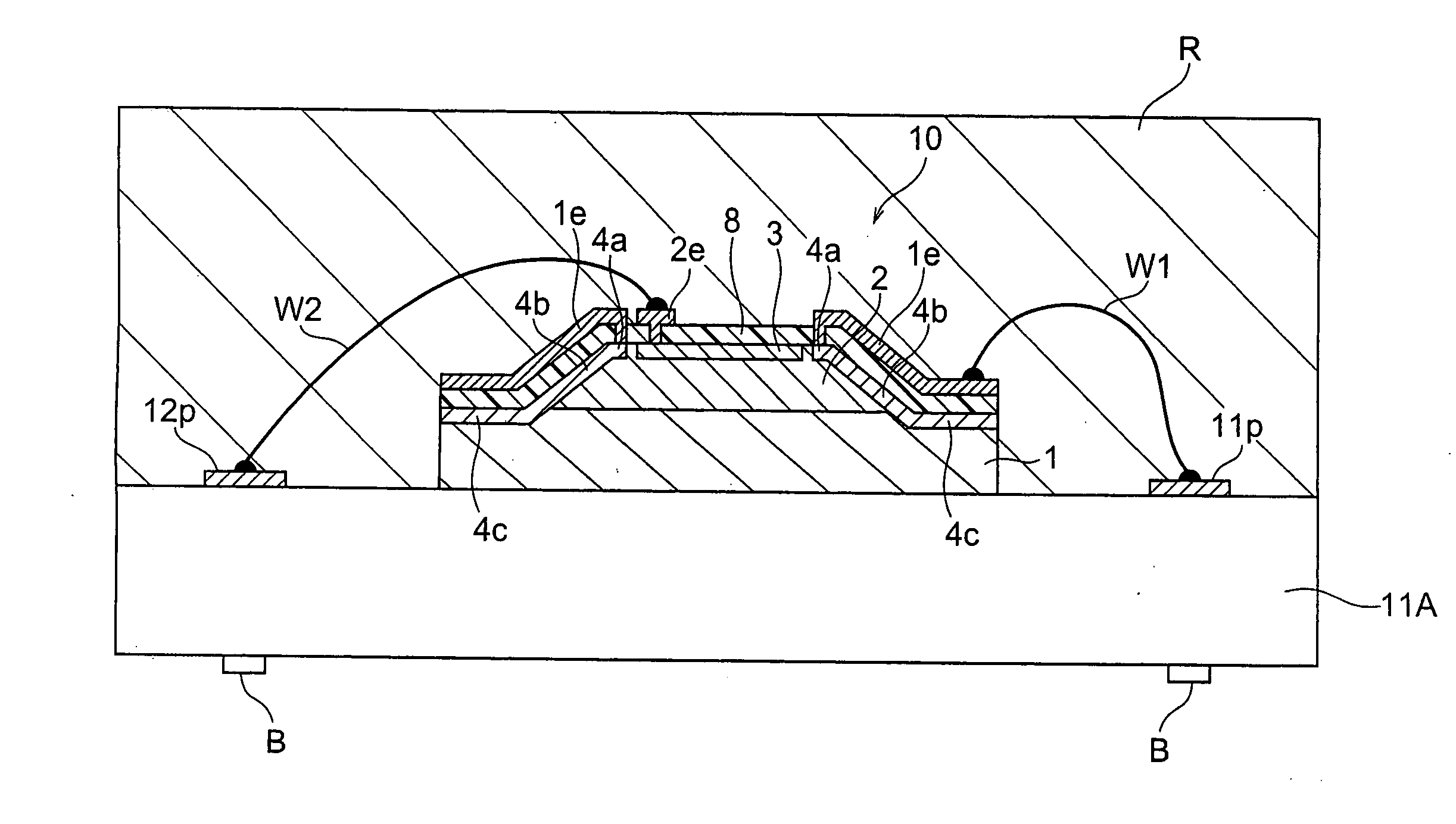
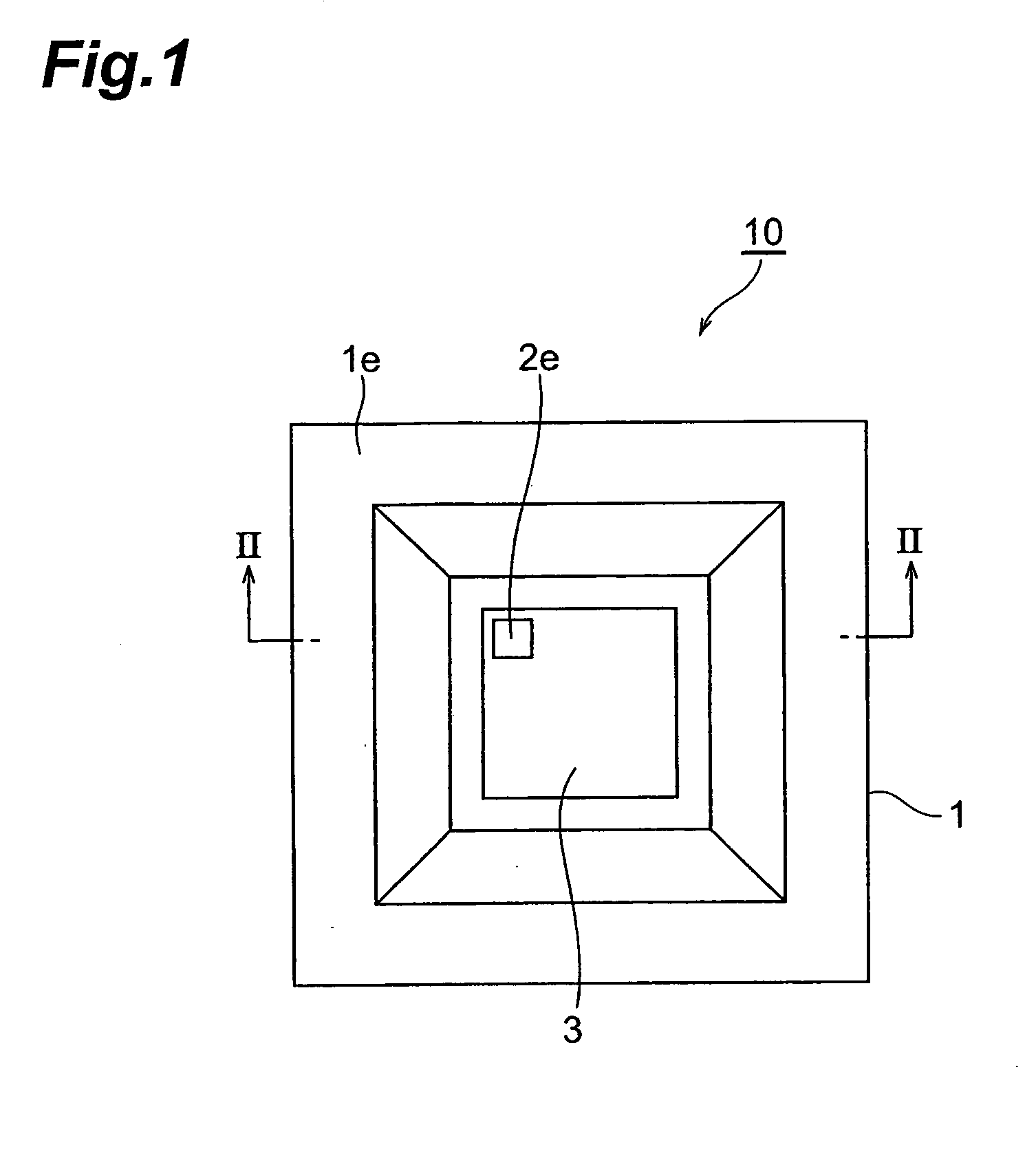
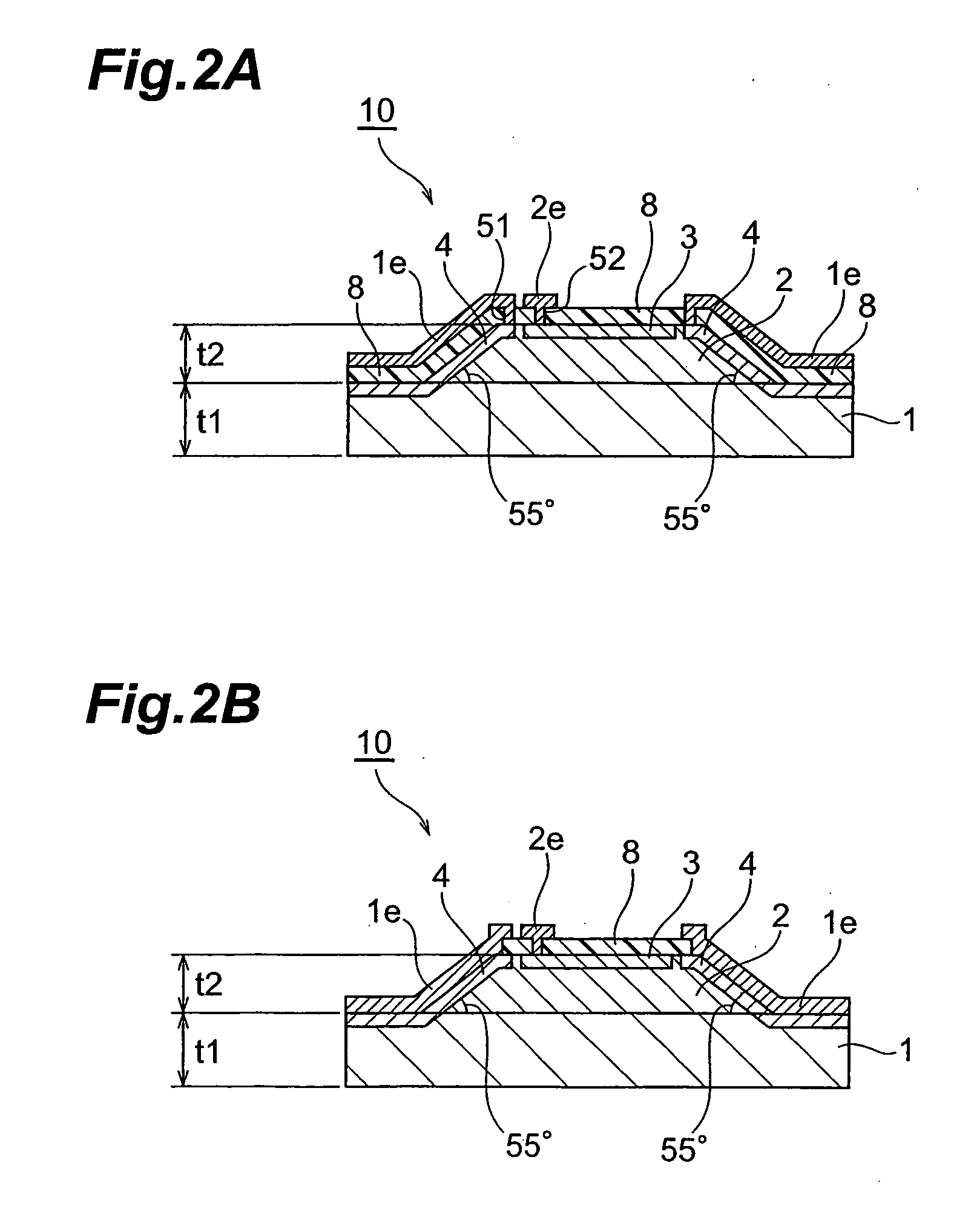
[0033]FIG. 1 is a plan view of a photodetector according to an embodiment. FIG. 2A is a sectional view taken on arrows II-II of the photodetector shown in FIG. 1.

[0034] This semiconductor photodetector 10 has an N-type (first conductive type) first semiconductor substrate 1 of low resistivity, an N-type second semiconductor substrate 2 of high resistivity, and a P-type (second conductive type) impurity-added region (semiconductor region) 3. Here, “high resistivity” and “low resistivity” shall signify a relative relationship between resistivities. That is, second semiconductor substrate 2 has a higher resistivity than first semiconductor substrate 1. The impurity concentration is relatively low in the case of high resistivity and the impurity concentration is relatively high in the case of low resistivity.

[0035] The resistivity of first semiconductor substrate 1 is, for example, approximately 0.001 Ω·cm. The resistivity of second semiconductor substrate 2 is, for example, approxima...


PUM


Abstract

A semiconductor photodetector 10 has a first semiconductor substrate 1 that is of a first conductive type and a low resistivity and has a (111) front surface, and a second semiconductor substrate 2 that is of the first conductive type and a high resistivity, has a (100) front surface, and is adhered onto first semiconductor substrate 1. A semiconductor region 3 of a second conductive type is formed on the front surface side of second semiconductor substrate 2. A region of a periphery of semiconductor region 3 is etched until first semiconductor substrate 1 is exposed. A first electrode 1e and a second electrode 2e are electrically connected to the exposed front surface of first semiconductor substrate 1 and to semiconductor region 3, respectively.

Description

BACKGROUND OF THE INVENTION [0001] 1. Field of the Invention [0002] The present invention relates to a semiconductor photodetector and a photodetecting device. [0003] 2. Related Background Art [0004] High-speed response characteristics are being demand more than ever in recent years in the field of optical semiconductor devices, and especially photodetectors. Demands for high-speed response, high S / N ratio, low cost, etc., for various wavelengths of light emitting devices are becoming stronger especially with photodetectors for information communication that send and receive large volumes of information. [0005] For example, Patent Document 1 discloses a PIN photodiode for optical communication that is equipped with high-speed response characteristics. With this PIN photodiode, an N-type semiconductor region of high resistivity is epitaxially grown on an N-type semiconductor substrate of low resistivity. In this N-type semiconductor region (epitaxial layer), a photodetecting region i...

Claims


Application Information

Patent Timeline
Patent Type & Authority Applications(United States)
IPC IPC(8): H01L31/0203H01L31/10H01L31/0392H01L31/103
CPCH01L31/0203H01L31/0392H01L31/103Y02E10/50H01L2224/48464H01L2224/49107H01L2924/3025H01L2224/48227H01L2224/48091H01L2924/00014H01L2924/00H01L2924/10155
Inventor FUJII, YOSHIMAROOKAMOTO, KOUJISAKAMOTO, AKIRA
Owner HAMAMATSU PHOTONICS KK
Why Eureka
Try Eureka