Method for attaching dice to a package and arrangement of dice in a package

a technology for semiconductor devices and dice, applied in semiconductor devices, semiconductor/solid-state device details, electrical devices, etc., can solve the problems of reducing productivity, damage to the active surface, and inability of the interposer to attach dice to the package, so as to increase the productivity of die packaging

Inactive Publication Date: 2006-11-30
INFINEON TECH AG
View PDF9 Cites 29 Cited by
  • Summary
  • Abstract
  • Description
  • Claims
  • Application Information

AI Technical Summary

Benefits of technology

[0013] In one aspect, the invention increases the productivity of die packaging by attaching the interposer in the wafer level process without endangering any functionality of the dice.
[0023] With this method all dice are processed at the same time and under the same conditions. The dice are diced from the active side avoiding damaging the structure of the dice. Furthermore, no additional spacer-attach process at die level is necessary and the second die (daughter die or top die) can be attached immediately after the wire bonding process of the bottom die (mother die). Generally the die-attach process stability is improved.
[0027] Embodiments of the invention save silicon spacer and glue material. Furthermore, it is another advantage that a larger throughput due to a simplified die-attach process can be achieved.

Problems solved by technology

Arranging the interposers or the spacers in the die level reduces the productivity.
In addition, this interposer is not suitable for attaching dice to a die package because it is configured as a package substrate interconnecting to the exterior of the package.
The dicing of the wafer in the disclosed manner could cause damaging on the active surface.

Method used


Image

  • Method for attaching dice to a package and arrangement of dice in a package
  • Method for attaching dice to a package and arrangement of dice in a package
  • Method for attaching dice to a package and arrangement of dice in a package

Examples


Embodiment Construction

[0046] The making and using of the presently preferred embodiments are discussed in detail below. It should be appreciated, however, that the present invention provides many applicable inventive concepts that can be embodied in a wide variety of specific contexts. The specific embodiments discussed are merely illustrative of specific ways to make and use the invention, and do not limit the scope of the invention.

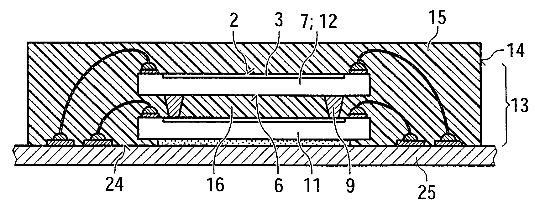
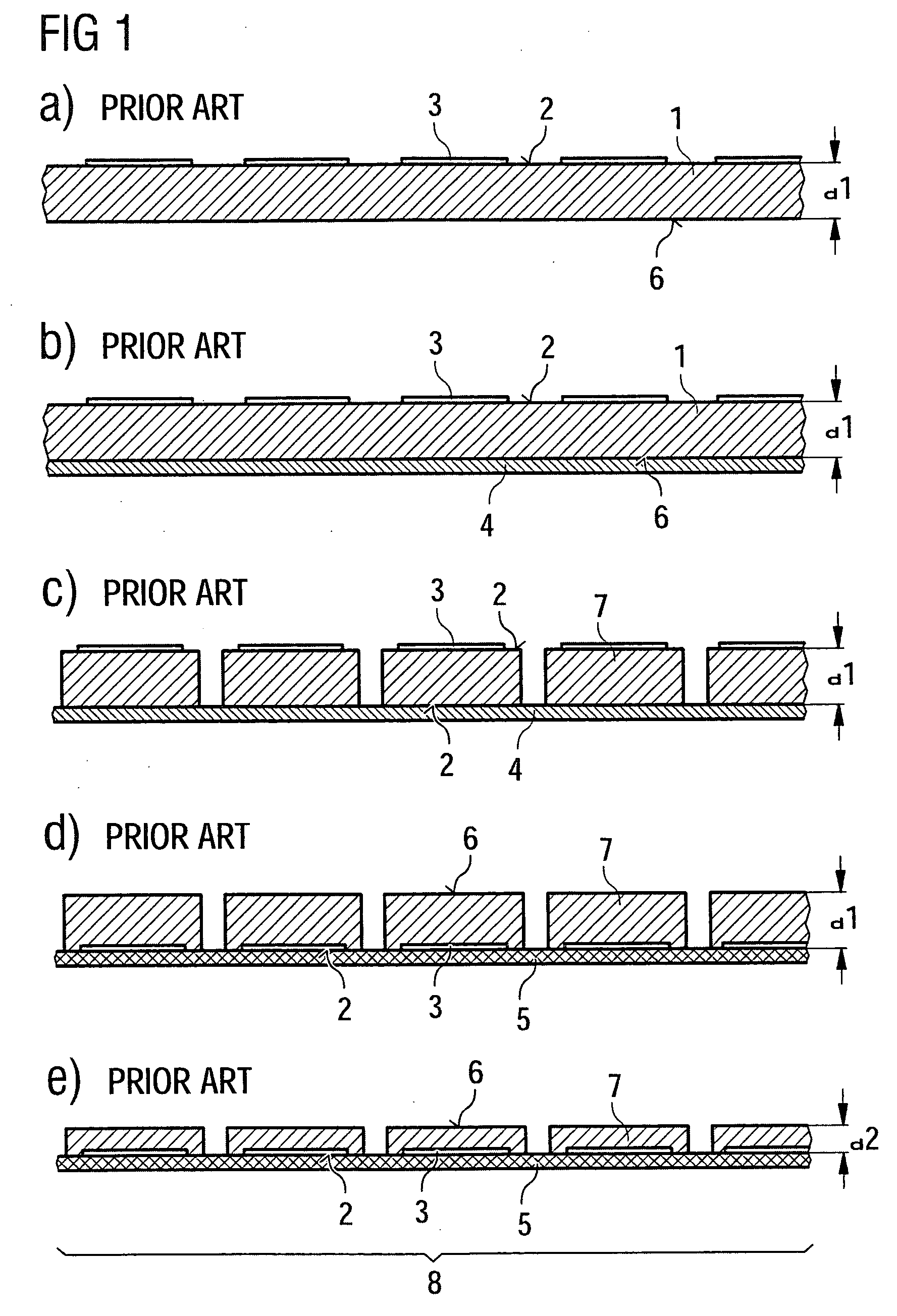
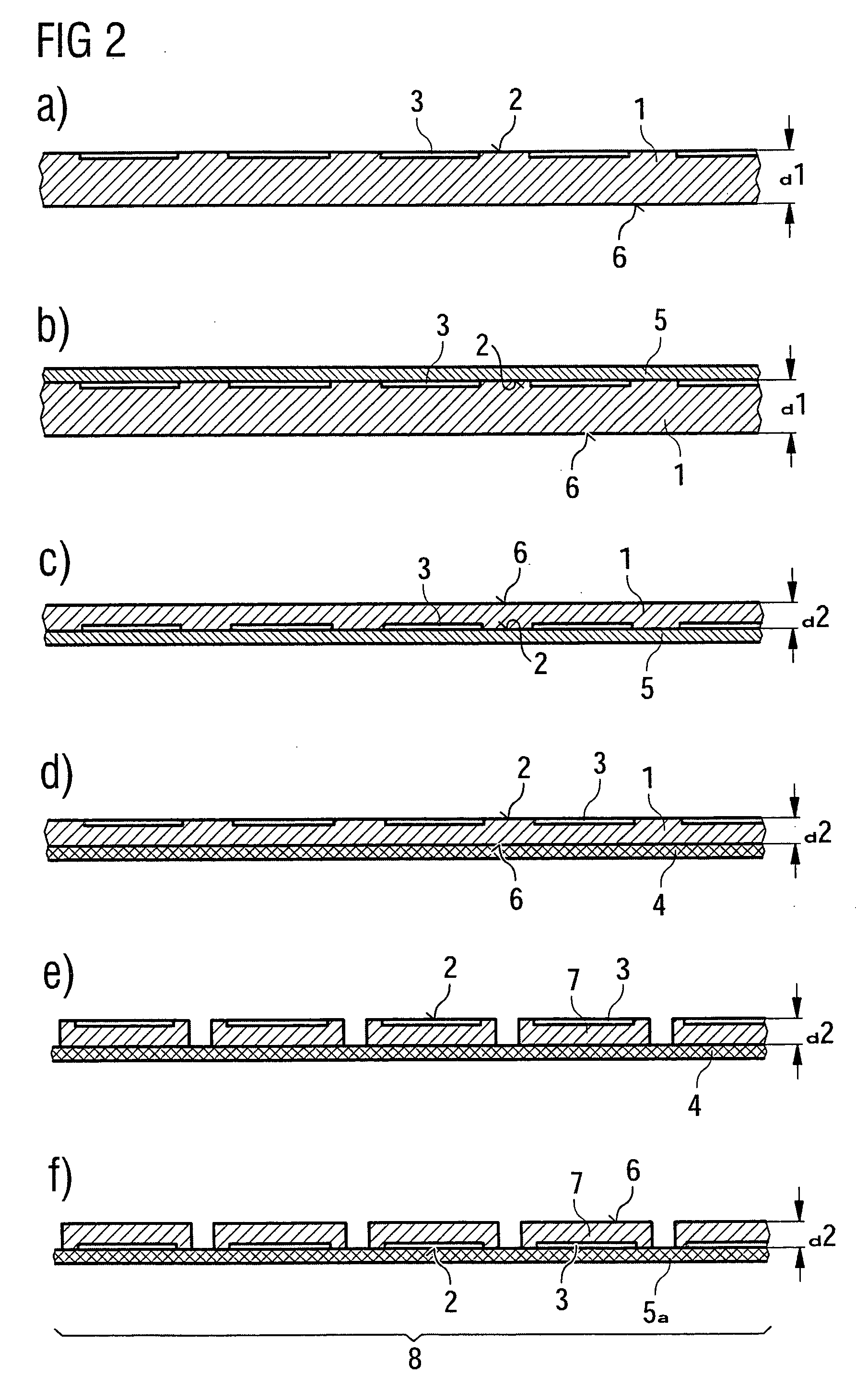
[0047] As illustrated in FIG. 1a, a wafer 1 is provided with an active surface 2 with a schematically shown redistribution layer 3. FIG. 1a illustrates the dicing before grinding process. In FIG. 1b the backside 6 is provided with a dicing tape 4. Thereafter, as shown in FIG. 1c, the wafer 1 is diced into multiple dice 7. After dicing, the dicing tape 4 is removed and a grinding tape 5 is added to the active surface 2 of the wafer 1, as shown in FIG. 1d. This grinding tape 5 protects the active surface 2 in the following grinding process. The backside 6 is grinded. Within t...


PUM


Abstract

The invention relates to a method and arrangement for assembling and packaging single and multiple semiconductor dice with an intermediate arranged interposer. The interposer is arranged onto the backside of a die within the wafer composite and thereby during the wafer level process. Preferably the interposer is printed by a stencil printing process.

Description

TECHNICAL FIELD [0001] The invention relates to method and arrangement for assembling and packaging single and multiple semiconductor dice with an intermediate arranged interposer. BACKGROUND [0002] For assembling a package of dice, at least one die is mounted on a package substrate by arranging an adhesive material intermediate the package and the die. Increasingly, a second die is positioned onto the top of the first die. In the same way, further dice can be mounted on the second die. [0003] In a standard process, the bond pads on a die are connected to contact pads on the substrate by wires bonded on the bond pads and the contact pads. In contrast thereto flip-chip technology connects the bond pads with the contact pads by solder bumps conductive adhesive. Therefore, the die is turned around so that its active surface is opposite to the upper surface of the substrate. Furthermore, the bond pads are opposite to the contact pads respectively. Solder balls are arranged either on the...

Claims


Application Information

Patent Timeline
Patent Type & Authority Applications(United States)
IPC IPC(8): H01L21/00
CPCH01L21/6835H01L21/6836H01L2224/32225H01L2224/32145H01L24/29H01L2924/014H01L2924/01033H01L2924/01006H01L2924/01005H01L2225/06575H01L2225/0651H01L2224/838H01L2224/83191H01L2224/73265H01L2224/48464H01L2224/48227H01L2224/48091H01L2224/32014H01L2221/68368H01L23/3121H01L24/27H01L24/83H01L25/0657H01L25/50H01L2221/68327H01L2221/6834H01L2221/68354H01L2924/00014H01L2924/00H01L2924/00012H01L2924/181H01L24/73
Inventor TROVARELLI, OCTAVIOMUELLER, SEBASTIAN
Owner INFINEON TECH AG
Why Eureka
Try Eureka