Capacitive array

a technology of capacitance arrays and arrays, applied in the field of capacitance arrays, can solve the problems of low operating speed of arrays and relative high stray capacitance, and achieve the effect of either finger distribution or distribution

Active Publication Date: 2006-11-30
STMICROELECTRONICS SRL
View PDF12 Cites 16 Cited by
  • Summary
  • Abstract
  • Description
  • Claims
  • Application Information

AI Technical Summary

Benefits of technology

[0027] Advantageously, the value of each capacitive entity is chosen to be equal to the smallest capacitive entity value multiplied by an integer power of two. Thus, the distribution of the fingers either si

Problems solved by technology

The fabrication constraints impose a relatively large minimum distance between the blocks, so the capacitive arrays of the prior art occupy a relatively large area because of the number of blocks.
Furthermore, the capacitive arrays according to the prior ar

Method used


Image

  • Capacitive array
  • Capacitive array
  • Capacitive array

Examples


first embodiment

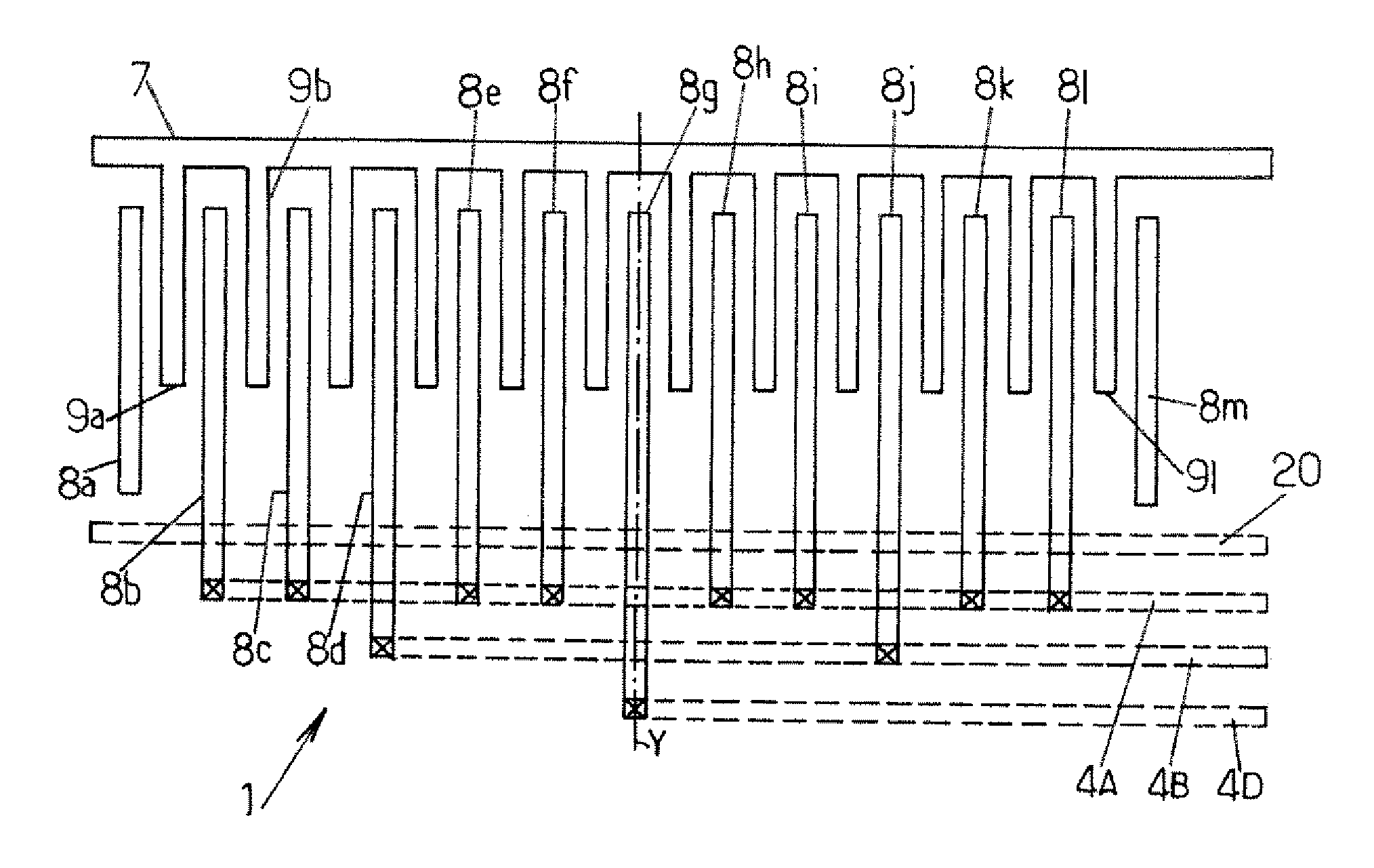
[0045] The first connecting track 4A, the second connecting track 4B and the third connecting track 4D form a set of connecting tracks. In the first embodiment, this set of connecting tracks extends in the plane of the substrate layer. Naturally, these connecting tracks 4A, 4B and 4D may create stray capacitances. However, these connecting tracks 4A, 4B and 4D are located relatively far away from the elements involved in the operation of the array, that is, the teeth and the fingers. Consequently, these stray capacitances have relatively little effect on the operation of the capacitive array.

[0046] On implementation, the connecting tracks 4A, 4B and 4D are located outside the block in which the comb 7 and the fingers 8a, . . . , 8m are integrated.

[0047] As is shown in FIGS. 6A, 6B and 6C, the capacitive array may comprise the substrate layer and one or more additional substrate layers. In this case, the set of connecting tracks may belong to one and the same plane. The set of conne...

second embodiment

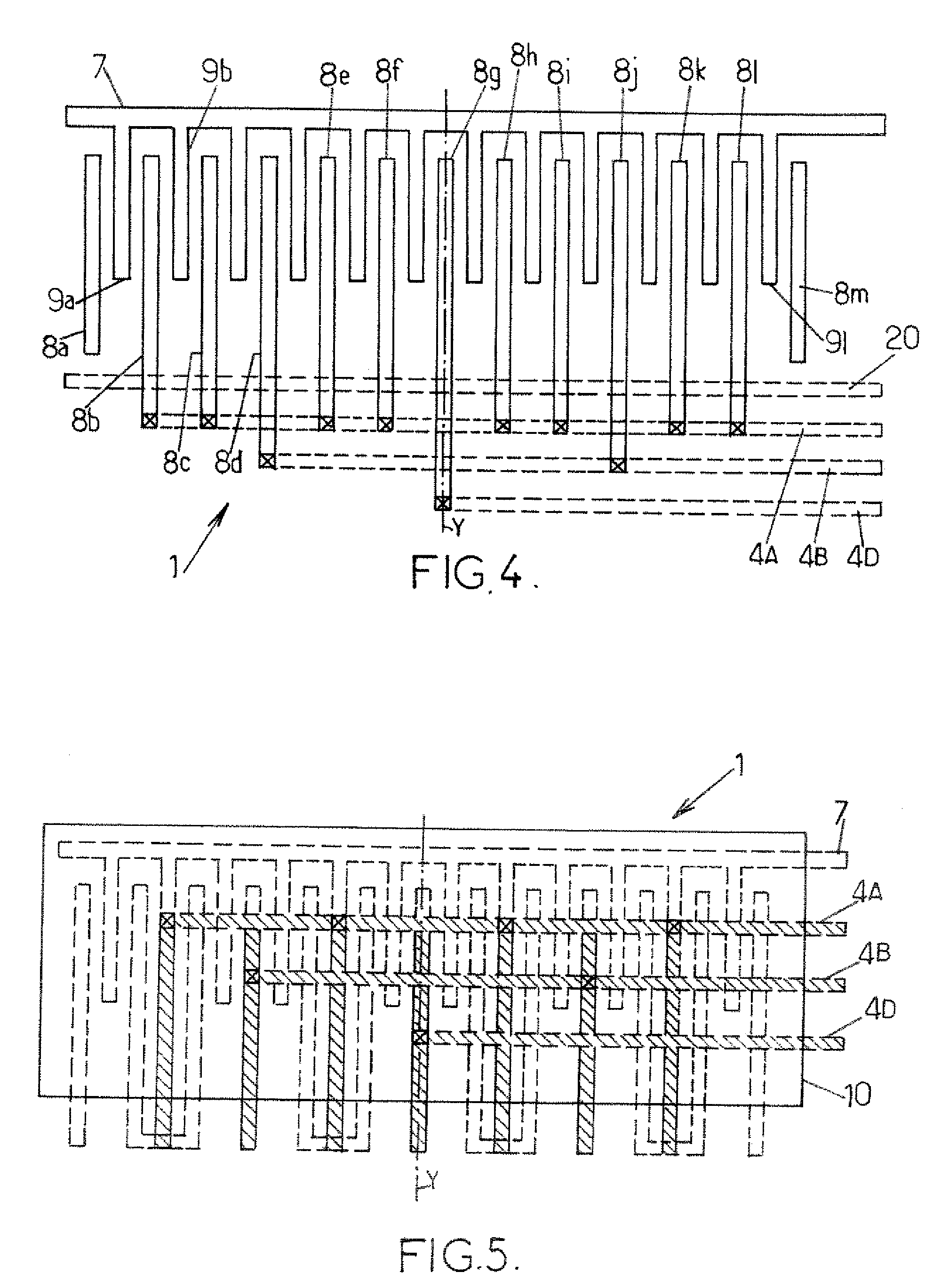
[0051]FIG. 5 shows an example of capacitive array according to the present invention. Just like the capacitive array represented in FIG. 4, the capacitive array represented in FIG. 5 has three capacitive entities presenting the same ratios of capacitance values. Each capacitive entity has fingers nested between the teeth of a comb 7. The fingers and the teeth of the comb 7 belong to one and the same substrate layer.

[0052] In a second embodiment, the capacitive array 1 also has a set of connecting tracks 4A, 4B and 4D above the substrate layer. A surface screen element 10 allows to insulate the substrate layer from the connecting tracks 4A, 4B and 4D. Thus, the stray capacitances generated by the connecting tracks 4A, 4B and 4D have relatively little effect on the ratios of the values of the capacitive entities. This surface screen element 10 may be substantially flat. The surface screen element 10 may be made of metal, for example of aluminium or copper. The surface screen element m...

third embodiment

[0056]FIGS. 6A, 6B and 6C are three views of an example of a capacitive unit of a capacitive array according to the present invention. FIG. 6A is a plan view, FIG. 6B is a perspective view and FIG. 6C is a side view. These three figures will be explained together.

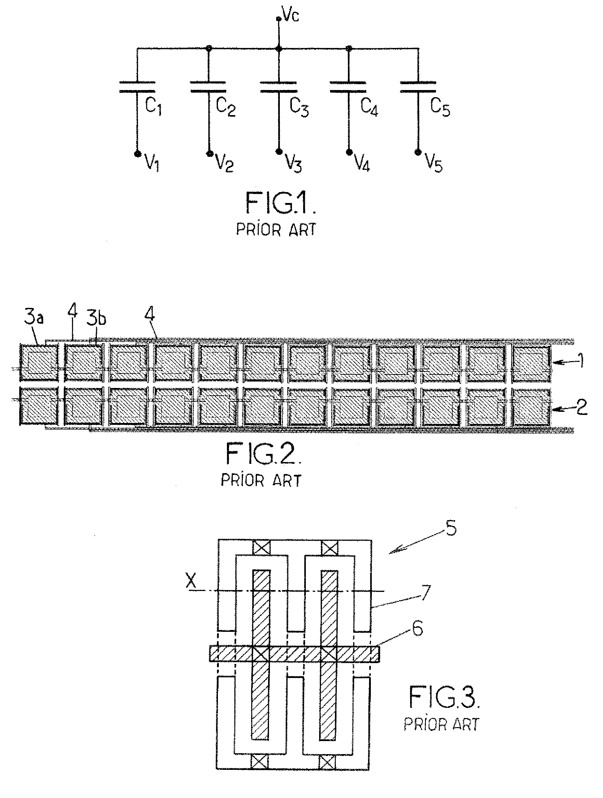
[0057] A capacitive array comprises a number of capacitive entities of different values. Each capacitive entity comprises at least one capacitive unit 13. The capacitive entities are constructed from capacitive units. Each capacitive entity is made up of a whole number of capacitive units,

[0058] The capacitive unit 13 comprises two teeth 9a1 and 9b1 of a comb 71 and a finger 81 nested between these teeth 9a1 and 9b1. This comb 71 and this finger 81 belong to a given substrate layer. For each capacitive entity, this substrate layer comprises a set of fingers. Advantageously, each set of fingers is constructed from a basic element with just one finger.

[0059] As illustrated in FIGS. 6A and 6C, the teeth 9a1 and 9b1 and the f...


PUM


Abstract

A capacitive array comprising at least two capacitive entities, comprising a substrate layer. The substrate layer comprises a comb comprising at least four substantially identical teeth, and, for each capacitive entity, a set of fingers comprising one or more interlinked fingers. At least two sets of fingers comprise a different number of fingers, each finger being nested between two teeth of the comb and being substantially identical to the other fingers. The fingers of each set of fingers are substantially distributed symmetrically relative to a median axis of the comb. The comb and the fingers are integrated in a single block.

Description

RELATED APPLICATION [0001] The present application claims priority of French Patent Application No. 05 05267 filed May 25, 2005, which is incorporated herein in its entirety by this reference. FIELD OF THE INVENTION [0002] The invention relates to the field of capacitive arrays. BACKGROUND OF THE INVENTION [0003] Capacitive arrays, also called arrays with charge distribution, are routinely used in various applications, for example in analogue to digital converters (ADC). A capacitive array comprises at least two capacitive entities of different values. [0004]FIG. 1 shows an example of capacitive array. The capacitive array 1 comprises a number of capacitive entities (C1, C2, C3, C4, C5). Each capacitive entity (C1, C2, C3, C4, C5) has a first terminal and a second terminal. The first terminals of the capacitive entities (C1, C2, C3, C4, C5) are interlinked. The reference Vc denotes the electrical potential at the first terminals of the capacitive entities (C1, C2, C3, C4, C5). The s...

Claims


Application Information

Patent Timeline
IPC IPC(8): H01L21/8242H01L29/94
CPCH01G4/38H01L28/60H01L27/0805H01L23/5223H01L2924/0002H01L2924/00
Inventor BACH, JEROME
Owner STMICROELECTRONICS SRL
Why Eureka
Try Eureka