

Three-axis integrated MEMS accelerometer
- Summary
- Abstract
- Description
- Claims
- Application Information
AI Technical Summary
Benefits of technology
Problems solved by technology
Method used
Image

Examples
second embodiment
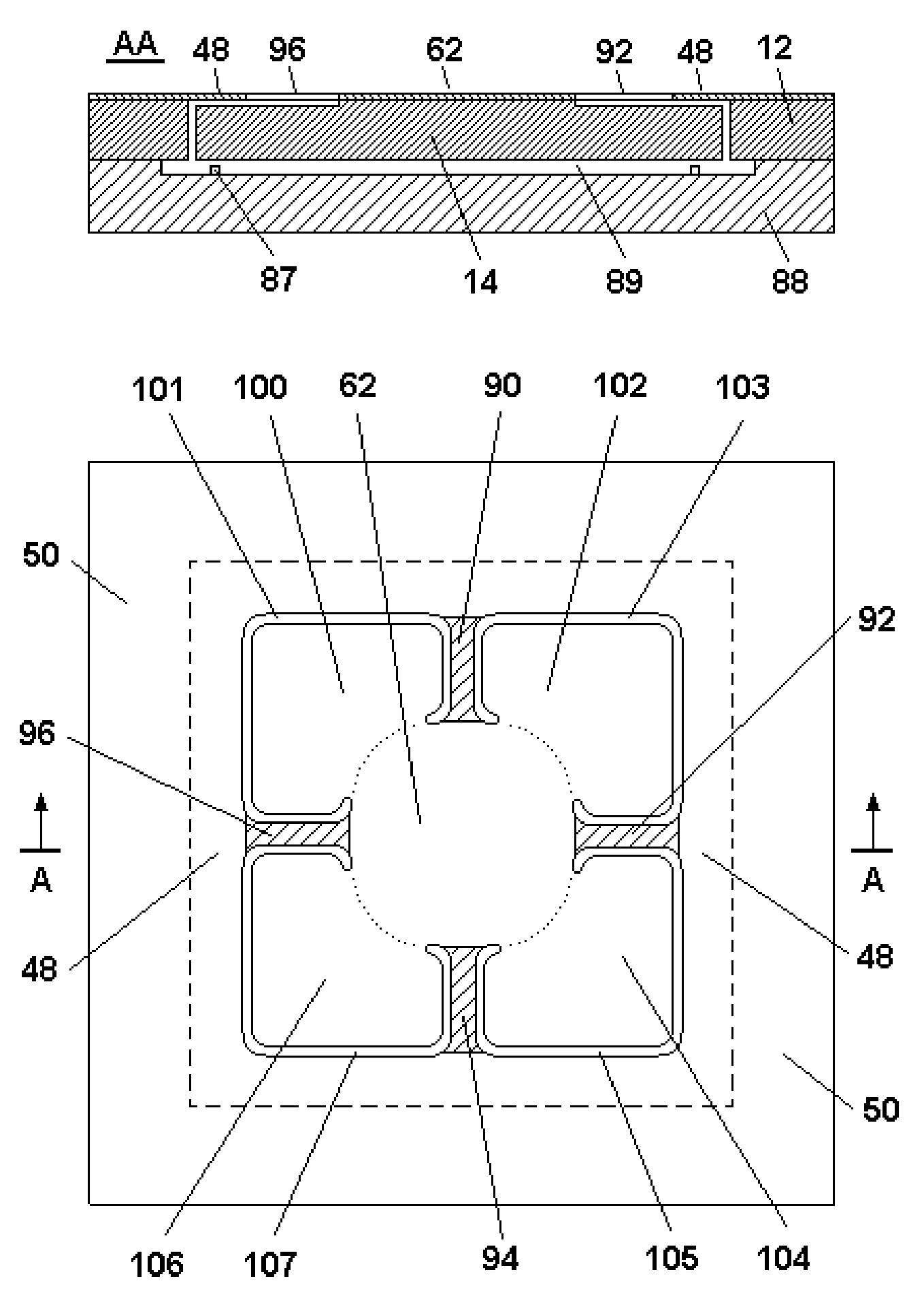
[0126]FIG. 2 shows mechanical structure of three-axis accelerometer according to the The sensor die 10 is fabricated on a semiconductor substrate of SOI type having handle layer 68 and device layer 70. A buried cavity 66 is formed in the handle layer 68 at the interface of the handle and device layers. Mechanical structure of the three-axis accelerometer consists of a frame, a proof mass 14 and an elastic element or suspension in the form of four beams 40, 42, 44, and 46. The frame has a thick portion 12 and a thin portion 48 having uniform thickness. The proof mass is separated from the thick portion 12 of the frame by a slot 13 and from the thin portion 48 of the frame by the buried cavity 66. Each of the four beams forming the elastic element has one end connected to the proof mass 14 in the connection area 62. The other end of each of the four beams is connected to the thin portion 48 of the frame. Beams 40, 42, 44, and 46 are separated from the thin portion 48 of the frame wit...
third embodiment
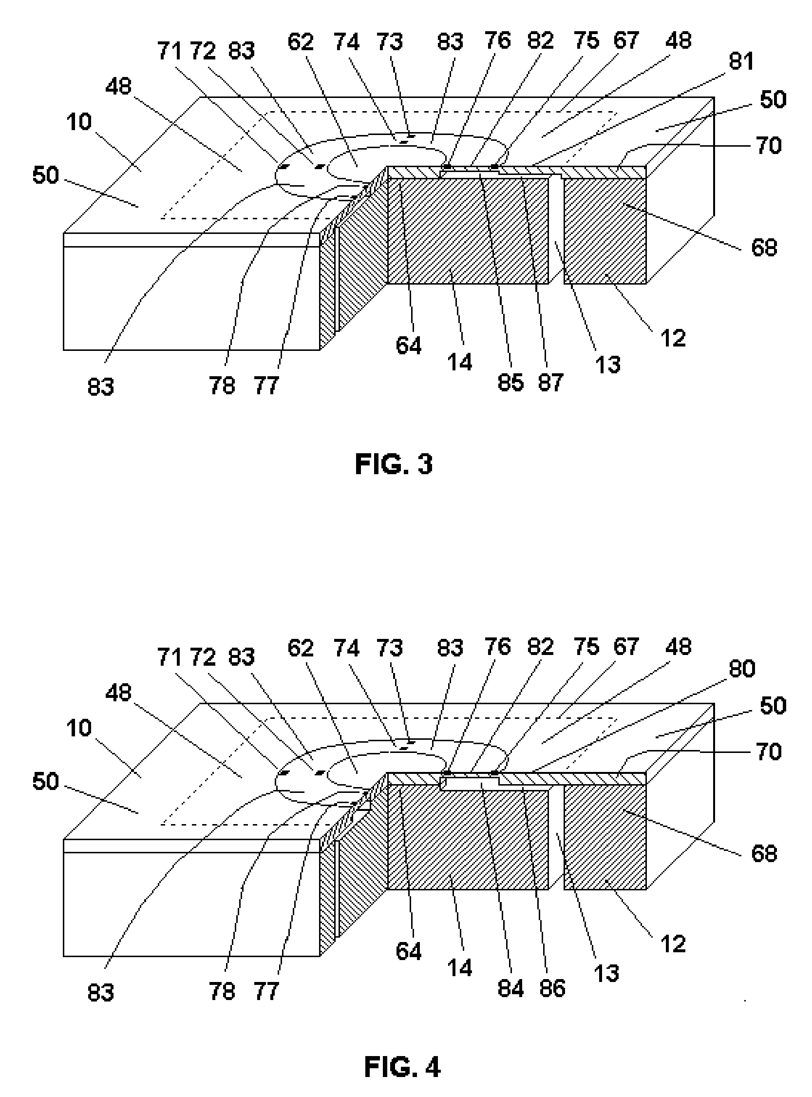
[0136]FIG. 3 and FIG. 4 show mechanical structures of three-axis accelerometer according to the
[0137] The sensor die 10 of three-axis accelerometer shown in FIG. 3 is fabricated on a semiconductor substrate of SOI type having handle layer 68 and device layer 70. A buried cavity 85, 87 are located in the device layer 70 at the interface of the handle and device layers. Mechanical structure of the three-axis accelerometer consists of a frame, a proof mass 14 and an elastic element in the form of an annular diaphragm 83. The frame has a thick portion 12 and a thin portion 48 having uniform thickness. The proof mass is separated from the thick portion 12 of the frame by a slot 13 and from the thin portion 48 of the frame by the buried cavity 85, 87. The annular diaphragm 83 is connected to the thin portion 48 of the frame on its outer edge and to the proof mass 14 at its inner edge. Alternatively, the elastic element can be formed as a set of beams (similar to the structure described in...
fourth embodiment
[0144]FIG. 5 shows mechanical structure of three-axis accelerometer according to the The sensor die 10 is fabricated on a semiconductor substrate of SOI type having handle layer 68 and device layer 70. A buried cavity 86 is formed at the interface of the handle and device layers. Mechanical structure of the three-axis accelerometer consists of a frame, a proof mass 14 and an elastic element in the form of a portion 82 of diaphragm 80. The frame has a thick portion 12 and a thin portion 48 having uniform thickness. The proof mass 14 is separated from the thick portion 12 of the frame by a slot 13 and from the thin portion 48 of the frame by the buried cavity 86. Stress-sensitive components 72, 74, and 76 are located on the elastic element 82.
[0145] The improvement made to the three-axis accelerometer according to the fourth embodiment is related to simplification of the structure and as a result of that decrease of its cost.
[0146] As it can be seen from FIG. 5, the proof mass is su...
PUM
 Abstract
Description
Claims
Application Information