Side-emitting LED package and method of manufacturing the same

a technology of led chips and side-emitting, which is applied in the direction of basic electric elements, electrical equipment, semiconductor devices, etc., can solve the problems of low productivity per hour, method is not effective in allowing light from led chips, and thickness is quite larg

Inactive Publication Date: 2006-12-07
SAMSUNG ELECTRO MECHANICS CO LTD
View PDF4 Cites 84 Cited by
  • Summary
  • Abstract
  • Description
  • Claims
  • Application Information

AI Technical Summary

Benefits of technology

[0012] The present invention has been made to solve the foregoing problems of the prior art and it is therefore an object of the present invention to provide a side-emitting LED package which prevents light from being scattered upward beyond a reflective layer and effectively reflects light sideward, and a method of manufacturing the same.

Problems solved by technology

The high power package used for an LCD backlight unit adopts vertical side emission method in which a package with a heat slug mounted thereon is covered by a lens, which results in a problem of a quite large thickness.
However, the current trend is that slimmer LCD backlight units require slimmer LED packages therefor.
However, this method is not effective in allowing light from the LED chip 240 to be reflected on the reflective film and reflected sideward from the package.
Therefore, such a conventional structure is limited in emitting light sideward from a conventional upward direction, and the lead terminal results in low productivity per hour.
In this conventional structure, however, light is scattered upward, and thus is limited in effectively inducing light to be emitted sideward, and also has low productivity per hour owing to the lead terminal.

Method used


Image

  • Side-emitting LED package and method of manufacturing the same
  • Side-emitting LED package and method of manufacturing the same
  • Side-emitting LED package and method of manufacturing the same

Examples


Embodiment Construction

[0025] Preferred embodiments of the present invention will now be described in detail with reference to the accompanying drawings.

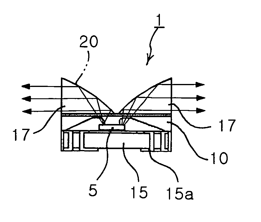
[0026] As shown in FIGS. 3 to 5, a side-emitting LED package 1 according to the present invention is for emitting light sideward from an LED chip as a light source 5 from the side of a molded part 10. The direction of light emission is preferably in parallel with a plane where the LED chip is mounted on.

[0027] The side-emitting LED package 1 according to the present invention has a substrate 15 with an electrode 15a formed thereon. The substrate 15 can preferably be a Printed Circuit Board (PCB) or a ceramic substrate with a pattern electrode or a vertical electrode 15a such as a via.

[0028] The LED chip 5(see FIG. 4) is mounted on the substrate 15 and electrically connected to the electrode 15a. The LED chip can be a horizontal type with electric terminals formed on an upper surface thereof and can also be a vertical type with electric terminals formed...


PUM


Abstract

The invention relates to a side-emitting LED package and a manufacturing method thereof. The side-emitting LED package includes a substrate with an electrode formed thereon, and a light source disposed on the substrate and electrically connected to the electrode. The side-emitting LED package also includes a molded part having an upper surface with a center thereof depressed concavely, covering and protecting the substrate and the light source, and a reflection layer covering an entire upper surface of the molded part to reflect light sideward from the molded part which forms a light transmitting surface. The package is not restricted in the shape of the molded part and is not affected by the LED chip size, enabling a compact structure. The invention can also process a substrate by a PCB process, enabling mass-production.

Description

CLAIM OF PRIORITY [0001] This application claims the benefit of Korean Patent Application No. 2005-46618 filed on Jun. 1, 2005, in the Korean Intellectual Property Office, the disclosure of which is incorporated herein by reference. BACKGROUND OF THE INVENTION [0002] 1. Field of the Invention [0003] The present invention relates to a side-emitting LED package for emitting light sideward, and a method of manufacturing the same. More particularly, the invention relates to a side-emitting LED package, which has a reflective layer easily manufactured into desired shapes for emitting light sideward, can be mass-produced in a compact size regardless of an LED chip size, and can have an LED array inside thereof, thereby significantly improving productivity, and a method of manufacturing the same. [0004] 2. Description of the Related Art [0005] Recently, an LED package has been increasingly adopted in an LCD backlight unit (LCD BLU). The high power package used for an LCD backlight unit ado...

Claims


Application Information

Patent Timeline
Patent Type & Authority Applications(United States)
IPC IPC(8): H01L33/00H01L33/54H01L33/50H01L33/56H01L33/60H01L33/62
CPCH01L25/0753H01L33/54H01L33/60H01L24/97H01L2924/1815H01L2224/48091H01L2924/00H01L2924/15787H01L2924/181H01L2924/12035H01L2924/12041H01L2924/00014
Inventor HAN, KYUNG TAEGCHOI, MYOUNG SOOLEE, SEON GOOHAHM, HUN JOOHAN, SEONG YEONSONG, CHANG HOPARK, YOUNG SAM
Owner SAMSUNG ELECTRO MECHANICS CO LTD
Why Eureka
Try Eureka