Flip-chip LED chip structure and manufacturing method thereof

A LED chip, flip-chip welding technology, applied in the direction of semiconductor devices, electrical components, circuits, etc., can solve the problems of reduced emission area, epitaxial layer structure damage, serious light loss, etc., to buffer the change of lateral stress and reduce Effects of intensifying lattice defects and prolonging service life

Inactive Publication Date: 2011-05-04
CHONGQING UNIV
View PDF5 Cites 41 Cited by
  • Summary
  • Abstract
  • Description
  • Claims
  • Application Information

AI Technical Summary

Problems solved by technology

[0008] This method has the following problems: Although ITO is transparent, it also has a certain reflection; because the electrode is made on the surface of the light exit, the light exit area is reduced; the production of the n-type electrode needs to etch a certain area The multi-quantum well layer reduces the light-generating area and generally affects the light-exit efficiency, close to offsetting the light-exit effect produced by roughening
[0012] This method has the following problems: the epitaxial layer structure may be damaged during peeling; this peeling method requires relatively high precision equipment; the above structure requires electrodes to be made on the n-GaN surface, which reduces the light output area ; Since the light exits from the n-GaN surface, a part of the light will be incident on the p-GaN layer, resulting in serious light loss

Method used


Image

  • Flip-chip LED chip structure and manufacturing method thereof
  • Flip-chip LED chip structure and manufacturing method thereof
  • Flip-chip LED chip structure and manufacturing method thereof

Examples


Embodiment 1

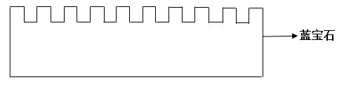
[0062] Example 1: see figure 1 with figure 2 , a flip-chip LED chip structure, including the epitaxial layer on the sapphire substrate and the SiO 2 / Si is the electrode layer of the substrate; the front of the sapphire substrate is etched with a periodic structure of circular hole-like hole 1 structure, the radius of the circular hole is 3 μm, the depth is 1 μm, and the period interval is 2.5 μm, the sapphire substrate The backside is etched with a random pattern;

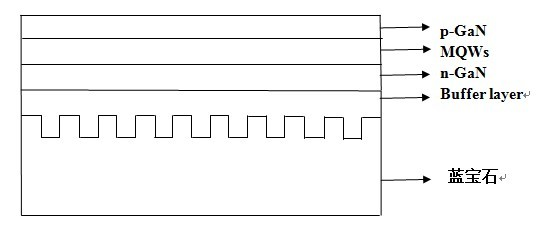
[0063] see image 3 , an epitaxial layer consisting of buffer layer buffer layer, n-type GaN layer n-GaN, multi-quantum well layer MQWs and p-type GaN layer p-GaN is grown on the front side of the sapphire substrate etched with round holes;

[0064] see Figure 4 with Figure 5 , taking the center line of the p-GaN p-GaN layer as the symmetry line, the two ends of the p-GaN layer p-GaN are symmetrically etched with cathode electrode grooves, and the etched epitaxial layer surface is divided into three part...

Embodiment 2

[0075] Example 2: see Figure 9 , the difference from Implementation 1 is that the periodic structural holes (1) etched on the front side of the sapphire substrate of the flip-chip LED chip structure are octagonal, and the side length of the octagon is 2 μm; the depth is 1 μm, and the period The pitch is 2.5 μm; the backside of the sapphire substrate is etched with a random pattern.

[0076] The manufacturing method of embodiment 2 is different from implementation 1 in that:

[0077] Step 1: On the polished sapphire substrate, use a laser to etch an octagon with a periodic structure, wherein the side length of the octagon is 2 μm; the depth is 1 μm, and the period interval is 2.5 μm. All the other steps are the same as in Example 1, omitted here.

Embodiment 3

[0078] Example 3: see figure 1 with figure 2 , a flip-chip LED chip structure, including the epitaxial layer on the sapphire substrate and the SiO 2 / Si is the electrode layer of the substrate; the front of the sapphire substrate is etched with a periodic structure of circular hole-like hole 1 structure, the radius of the circular hole is 3 μm, the depth is 1 μm, and the period interval is 2.5 μm, the sapphire substrate The backside is etched with a random pattern;

[0079] see image 3 , an epitaxial layer consisting of buffer layer buffer layer, n-type GaN layer n-GaN, multi-quantum well layer MQWs and p-type GaN layer p-GaN is grown on the front side of the sapphire substrate etched with round holes;

[0080] see Figure 10 with Figure 11, with the center line of the p-GaN layer p-GaN as the symmetry line, four cathode electrode grooves are etched symmetrically at the four corners of the p-type GaN layer p-GaN, and the etched epitaxial layer surface is divided into...


PUM


Abstract

The invention discloses a flip-chip LED chip structure and a manufacturing method thereof. The LED chip comprises an epitaxial layer taking sapphire as substrate and an electrode layer taking SiO2 / Si as substrate; holes of periodical structure are etched on the front surface of the sapphire substrate, and random patterns are etched on the back surface; a growth buffer layer, an n type GaN layer (n-GaN), an MQWs (multi quantum wells) layer and a p type GaN layer (p-GaN) are successively grown on the sapphire substrate etched with holes as the epitaxial layer; one or more negative electrode grooves are etched on the p type GaN layer (p-GaN); a p type contact layer is sputtered on the p type GaN layer (p-GaN); an n type ohmic contact layer is electroplated on the n type GaN layer (n-GaN) exposed after etching; titanium (Ti), platinum (Pt) and aurum (Au) are successively deposited on the SiO2 / Si substrate as an electrode layer; the electrode distribution on the electrode layer is coincident with that on the etched epitaxial layer; and the LED chip is formed by bonding the epitaxial layer on the front surface of the sapphire substrate and the electrode layer on the SiO2 / Si substrate with Au solder. The structure has the advantages of stable performance, high utilization rate of electric energy and long service life.

Description

technical field [0001] The invention relates to the technical field of light-emitting diode chips, in particular to a flip-chip soldered LED chip structure and a manufacturing method thereof. [0002] Background technique [0003] Under the urging of the global energy crisis, various energy-saving optoelectronic devices have emerged as the times require. Light-emitting diodes (LEDs), relying on their low energy consumption, no pollution, and long life, have gradually become the third-generation light source after incandescent lamps and fluorescent lamps. White LED lighting has low power consumption, which is 20% of incandescent lamps with the same lighting brightness and 50% of fluorescent lamps. It has unique advantages such as energy saving, environmental protection and green lighting. [0004] Although LED chips have been commercialized, the problem of low light extraction efficiency of LED chips has not been well resolved so far. At present, the luminous efficacy of c...

Claims


Application Information

Patent Timeline
Patent Type & Authority Applications(China)
IPC IPC(8): H01L33/20H01L33/22H01L33/38H01L33/46H01L33/00
Inventor 杜晓晴钟广明田健李小涛唐杰灵
Owner CHONGQING UNIV
Why Eureka
Try Eureka