Package for light emitting diode, light emitting device, and light emitting device manufacturing method

a technology packaging, which is applied in the manufacturing of semiconductor/solid-state devices, semiconductor devices, electrical devices, etc., can solve the problems of reducing the emission affecting the production efficiency of light emitting diodes, and damage to light emitting layers, etc., to achieve high reflectance, facilitate assembly, and reduce defects

Inactive Publication Date: 2011-02-17
CI KASEI COMPANY
View PDF1 Cites 39 Cited by
  • Summary
  • Abstract
  • Description
  • Claims
  • Application Information

AI Technical Summary

Benefits of technology

[0035]In accordance with the invention, the connection between the upper electrode of the vertical electrode type light emitting diode, the light emitting surface of which has fine ridges formed thereon, and the conductive member does not use wire bonding, so vibration is not imposed on the bonding portion and / or the light emitting layer, making it possible to obtain light emitting devices with few defects. The vertical electrode type light emitting diode having fine ridges formed on the light emitting surface not only reflects light efficiently, but does not need sealing resin, enabling the radiation of strong light.
[0036]In accordance with the invention, the ceramic molding or ceramic substrate comprising the package is formed of porous ceramic, so light reflected and diffused on the surface can be effectively utilized without forming a particular reflecting surface, enabling high reflectance.
[0037]In accordance with the invention, a light emitting diode package can be obtained by just fitting a conductive member in the ceramic molding or ceramic substrate having at least two openings, so there are few parts and assembly is facilitated, and the number of steps involved is reduced.
[0038]Since in accordance with the invention it is composed of a ceramic body in which a reflecting frame and an opening formed inside the reflecting framework are integrally formed, and a lead-shaped metal substrate that fits in the opening, assembly is easy, enabling a low cost light emitting diode package to be obtained.
[0039]In accordance with the invention, the upper electrode of the vertical electrode type light emitting diode and a lead-shaped connection substrate are connected by a ribbon-shaped metal member, so the size of the bonding area is increased and the connection can be made using solder, so heat dissipation property is good and a large current flow is possible.
[0040]In accordance with the invention, with just a few parts, that is, the reflecting frame, and a ceramic body having at least two openings to which a lead-shaped metal mounting substrate, a lead-shaped metal connection substrate and a metal member are connected, assembly is easy and the number of steps involved is reduced.

Problems solved by technology

With wire bonding, there is a risk of the light emitting layer being damaged from the ultrasonic vibration used to connect the wire to the light emitting diode.
Also, there is a risk of the wire bonding connection being broken by heat generated by the flow of a large current.
Moreover, in order to protect the light emitting layer of the light emitting diode and the wire bonding connection of the light emitting device, the package is packed with insulating material, but the insulating material causes a decrease in the emission efficiency of the light emitting diode.
Also, the strength of the adhesion between the insulating material and the metal substrates is a problem.

Method used


Image

  • Package for light emitting diode, light emitting device, and light emitting device manufacturing method
  • Package for light emitting diode, light emitting device, and light emitting device manufacturing method
  • Package for light emitting diode, light emitting device, and light emitting device manufacturing method

Examples


example embodiment 1

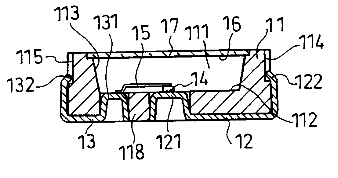
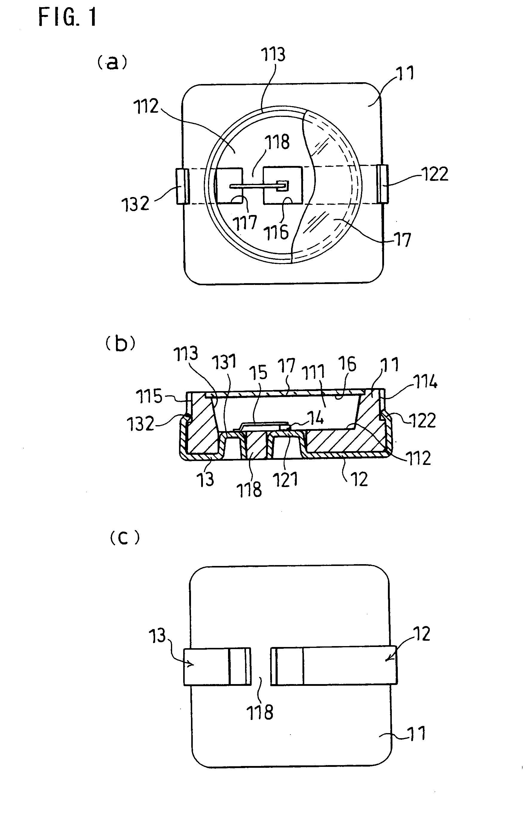
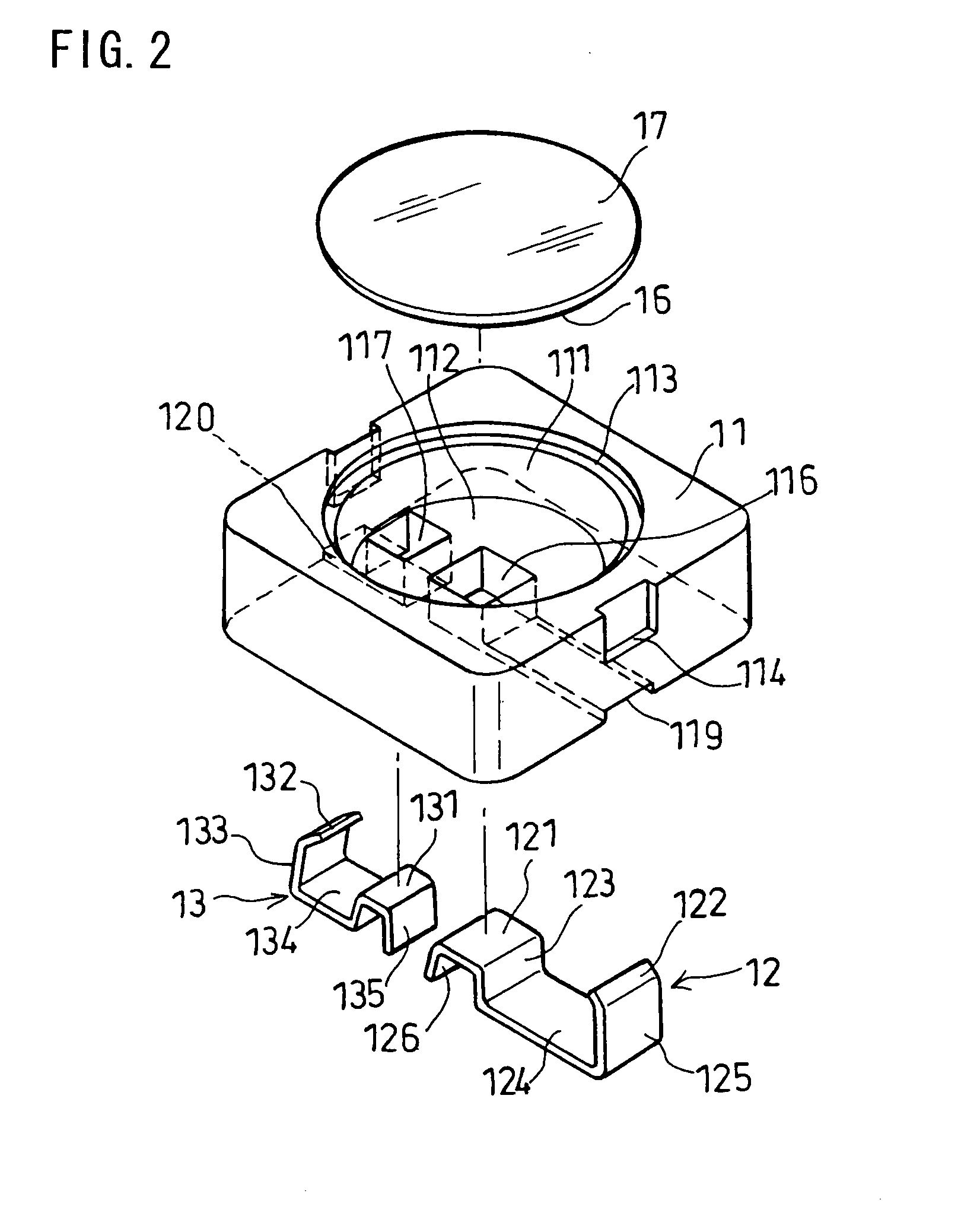
[0115]FIGS. 1(a) to (c) show a first example embodiment of the invention, with (a) being a plan view of the light emitting device, (b) being a cross-sectional view of the light emitting device, and (c) being a bottom view of the light emitting device. FIG. 2 is a perspective assembly view for explaining the light emitting diode package of the first example embodiment of the invention. In FIGS. 1(a) to (c) and FIG. 2, a light emitting diode package is comprised of at least a ceramic molding 11, and a first conductive member 12 and a second conductive member 13.

[0116]The ceramic molding 11 comprises a space 111 formed by a recessed portion, an inside bottom portion 112 that is the bottom portion of the space, a reflecting surface 113 formed around the inside bottom portion 112, a first opening 116 and a second opening 117 formed in the inside bottom portion 112, a first engaging portion 114 and a second engaging portion 115 formed at both ends, and recessed grooves 119 and 120 (see FI...

example embodiment 2

[0122]FIGS. 3(a) to (c) show a second example embodiment of the invention, with (a) being a plan view of the light emitting device, (b) being a cross-sectional view of the light emitting device, and (c) being a bottom view of the light emitting device. The points of difference between the light emitting device of the second example embodiment of FIGS. 3(a) to (c) and that of the first example embodiment are the ceramic substrate 31, and the hemispherical cover 32 with a fluorescent material containing film member 33 formed on the inside surface, provided over the ceramic substrate 31. The ceramic substrate 31 has a first opening 316 and a second opening 317 formed therein, and a first engaging portion 314 and a second engaging portion 315 formed at both ends.

[0123]The first conductive member 12 and the second conductive member 13, the first opening 316 and the second opening 317, the vertical electrode type light emitting diode 14, and the metal member 15 are the same as in the firs...

example embodiment 3

[0124]FIGS. 4(a) and (b) show a third example embodiment, of the invention, with (a) being a plan view of a light emitting device in which a plurality of vertical electrode type light emitting diodes are connected in series, and (b) is a cross-sectional view of the light emitting diode. In the third example embodiment of FIGS. 4(a) and (b), a plurality of the light emitting devices of the second example embodiment are connected in series on a single ceramic substrate 41. The first conductive member 12 and the fourth conductive member 13 of the second example embodiment are the same as those of the second example embodiment. A projecting portion provided at both ends of a second conductive member 45 and a third conductive member 46 fit in the respective openings.

[0125]Vertical electrode type light emitting diodes 14-1, 14-2, 14-3 are mounted on the projecting portions of the conductive members, and are bonded to the other projecting portions by metal members 15-1, 15-2, 15-3 and sold...


PUM


Abstract

The present invention relates to a light emitting diode package for mounting a light emitting diode, a light emitting diode device with the light emitting diode package mounting a vertical electrode type light emitting diode thereon and a manufacturing method for manufacturing the light emitting device.
The light emitting diode package of the invention comprises at least a molding, and a first clip 122 and a second clip 123 fitted on the molding. The molding has at least a first opening 1212 and a second opening 1213 formed in a bottom portion thereof. The molding also has a reflecting portion 1214 formed around the first opening 1212 and the second opening 1213 for reflecting light. The molding further has a fluorescent film member mounting portion 1113 formed integrally for mounting a fluorescent film member 116 in the opening of the reflecting portion 1214. The first clip 122 has a light emitting diode mounting projection formed substantially at the center portion thereof for mounting the light emitting diode and is made to engage resiliently with the molding at both ends thereof. The first clip 122 engages with the molding at both ends thereof. The second clip 123 has a bonding projection formed to engage resiliently with the molding at both ends thereof.

Description

TECHNICAL FIELD[0001]This invention relates to a light emitting diode package for mounting at least one light emitting diode thereon, a light emitting device, and a light emitting device manufacturing method. The invention relates to a light emitting diode package having a structure able to deliver a large current to the light emitting diode, a light emitting device, a light emitting device manufacturing method.[0002]The invention relates to a package for a light emitting diode comprising at least a substrate formed integrally inside a reflecting frame, an opening formed in the substrate, and a lead-shaped conductive member fitted in the opening, a light emitting device, and a light emitting device manufacturing method.[0003]The invention relates to a package for a light emitting diode that has good heat dissipation property and high reliability through which a large current can be run by using solder to bond electrodes of a vertical electrode type light emitting diode to a lead-sha...

Claims


Application Information

Patent Timeline
Patent Type & Authority Applications(United States)
IPC IPC(8): H01L33/60H01L33/48H01L33/62
CPCH01L33/486H01L33/62H01L2224/48247H01L2224/45144H01L2924/00H01L2924/00014
Inventor FUSHIMI, HIROSHI
Owner CI KASEI COMPANY
Why Eureka
Try Eureka