Semiconductor integrated circuit
a technology of integrated circuits and semiconductors, applied in the direction of semiconductor devices, semiconductor/solid-state device details, electrical apparatus, etc., can solve the problems of more malfunctions in the semiconductor integrated circuit, the power supply potential of the data circuit 620 is varied, and the clock jitter degradation, so as to prevent the clock signal wiring from being affected and the amount of clock signal jitter caused by crosstalk noise reduction
- Summary
- Abstract
- Description
- Claims
- Application Information
AI Technical Summary
Benefits of technology
Problems solved by technology
Method used
Image

Examples
first embodiment
of the Present Invention
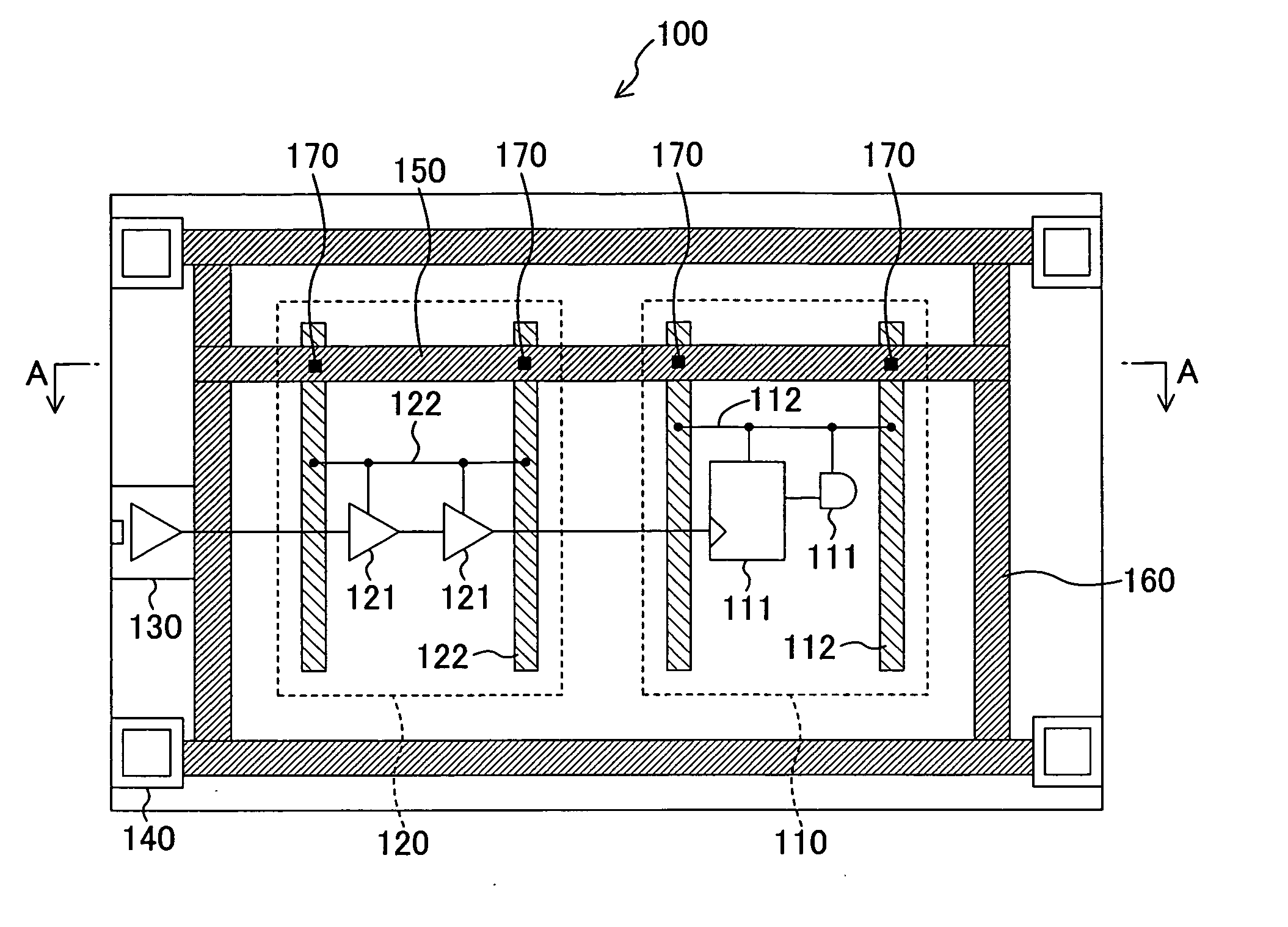
[0042]FIG. 1 is a block diagram showing the structure of a semiconductor integrated circuit 100 according to a first embodiment of the present invention. As shown in the figure, the substrate of the semiconductor integrated circuit 100 includes a data cell region 110 and a clock cell region 120, in which circuits are formed.
[0043] The data cell region 110 includes data circuits 111 and data circuit power supply wiring 112.
[0044] The data circuits 111 are composed of buffers, logic gates, flip flops, or the like and perform signal processing of an input signal.
[0045] The data circuit power supply wiring 112 provides the data circuits 111 with power supply voltage.
[0046] The clock cell region 120 includes clock circuits 121 and clock circuit power supply wiring 122.
[0047] The clock circuits 121 are composed of buffers, logic gates, flip flops, or the like and supply an input clock signal to the data cell region 110.
[0048] The clock circuit power supply wi...
second embodiment
of the Present Invention
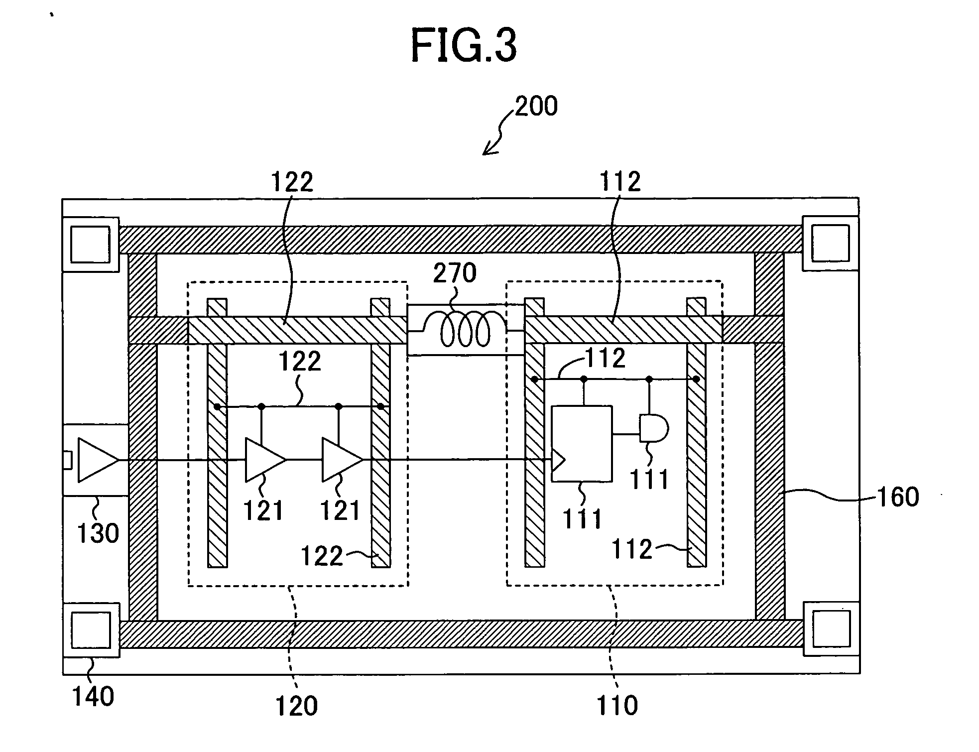
[0066]FIG. 3 is a block diagram showing the structure of a semiconductor integrated circuit 200 according to a second embodiment of the present invention. In the below-described embodiments, the components having the same function as those of the first embodiment and the like are designated by the same reference numerals and the description thereof will be thus omitted herein.
[0067] The semiconductor integrated circuit 200 is different from the semiconductor integrated circuit 100 of the first embodiment in that the data circuit power supply wiring 112 and the clock circuit power supply wiring 122 are connected with each other by a coil 270 instead of by the vias 170.
[0068] The coil 270 is an impedance element and a feature of the coil 270 is that the resistance component thereof is zero while the reactance component thereof has a finite value. It is well known that the resistance component of an impedance element typically causes a voltage drop for the dir...
third embodiment
of the Present Invention
[0076]FIG. 4 is a block diagram showing the structure of a semiconductor integrated circuit 300 according to a third embodiment of the present invention. The semiconductor integrated circuit 300 includes a data cell region 110, a first clock cell region 310, and a second clock cell region 320.
[0077] The semiconductor integrated circuit of this embodiment is different from the semiconductor integrated circuit of the first embodiment in that two clock signals are input into the semiconductor integrated circuit 300 through a first clock input terminal 330 and a second clock input terminal 340 and that the clock signal input through the first clock input terminal 330 is propagated by clock circuits 121 included in the first clock cell region 310 so as to be input into corresponding data circuits 111 in the data cell region 110 and the clock signal input through the second clock input terminal 340 is propagated by clock circuits 121 included in the second clock c...
PUM
 Abstract
Description
Claims
Application Information
 - R&D
- Intellectual Property
- Life Sciences
- Materials
- Tech Scout
- Unparalleled Data Quality
- Higher Quality Content
- 60% Fewer Hallucinations
Browse by: Latest US Patents, China's latest patents, Technical Efficacy Thesaurus, Application Domain, Technology Topic, Popular Technical Reports.
© 2025 PatSnap. All rights reserved.Legal|Privacy policy|Modern Slavery Act Transparency Statement|Sitemap|About US| Contact US: help@patsnap.com