CMOS image sensor pixel with selectable binning and conversion gain
- Summary
- Abstract
- Description
- Claims
- Application Information
AI Technical Summary
Benefits of technology
Problems solved by technology
Method used
Image

Examples
Embodiment Construction
[0024] Before discussing the invention in detail, it is instructive to clearly define CMOS active pixel sensor. CMOS refers to complimentary metal oxide silicon transistors in which complimentary means there are two transistors operating together which are composed of different dopants, one of n-type dopant and one of p-type dopant. The n-type dopant transistor is referred to as NMOS, and the p-type dopant transistor is referred to as PMOS. Active pixel sensors refer to electronic image sensors with active devices, such as transistors, that are associated with each pixel.
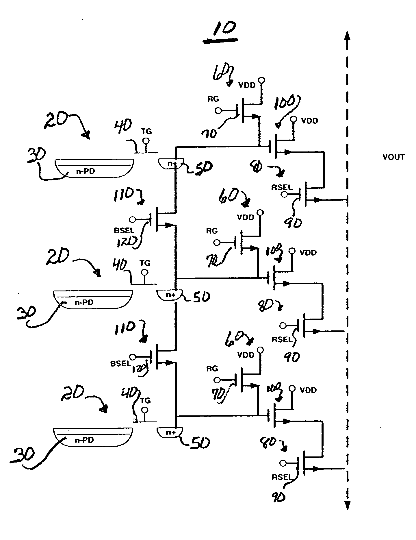
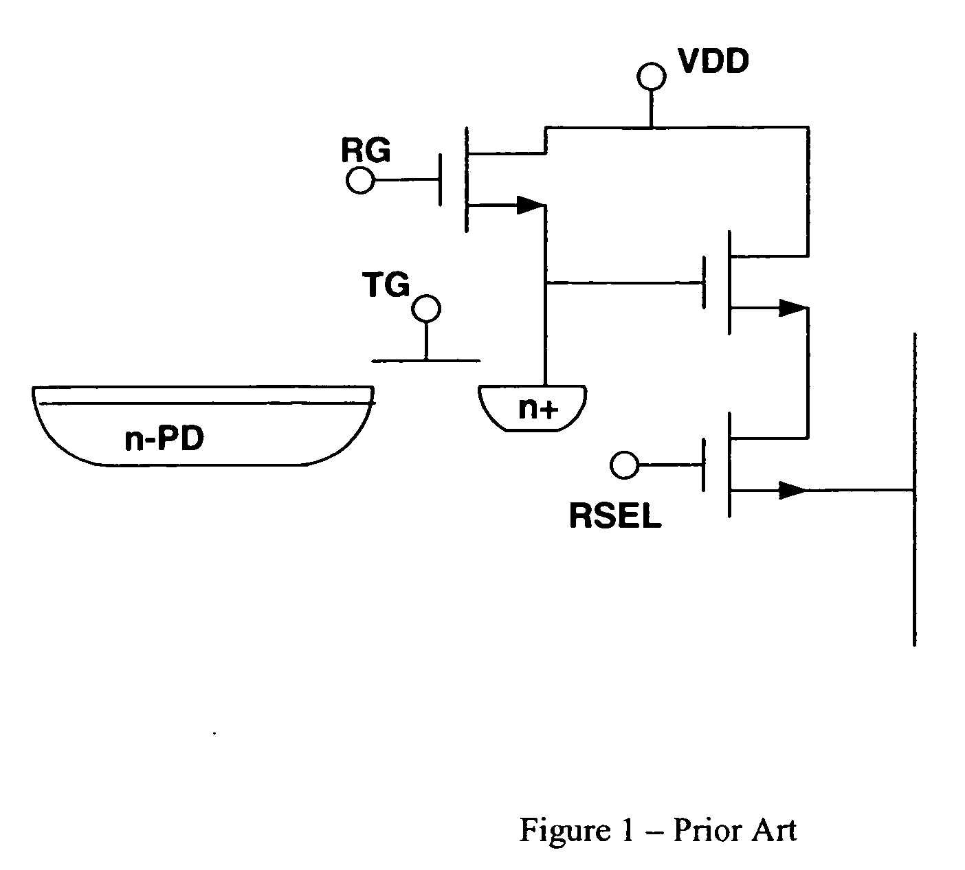
[0025] Now referring to FIG. 4, the CMOS active pixel image sensor 10 of the present invention is shown one embodiment of the present invention that enables charge domain binning in a selectable manner. As seen in FIG. 1, this is in its simplest embodiment a five-transistor pixel. Each pixel 20 includes a photodetector 30, preferably an n-type photodetector for capturing incident light that is converted into charge...
PUM
 Abstract
Description
Claims
Application Information
 - Generate Ideas
- Intellectual Property
- Life Sciences
- Materials
- Tech Scout
- Unparalleled Data Quality
- Higher Quality Content
- 60% Fewer Hallucinations
Browse by: Latest US Patents, China's latest patents, Technical Efficacy Thesaurus, Application Domain, Technology Topic, Popular Technical Reports.
© 2025 PatSnap. All rights reserved.Legal|Privacy policy|Modern Slavery Act Transparency Statement|Sitemap|About US| Contact US: help@patsnap.com