Infrared inspection apparatus, infrared inspecting method and manufacturing method of semiconductor wafer

a technology of infrared inspection and semiconductor wafer, which is applied in the direction of optical radiation measurement, semiconductor/solid-state device testing/measurement, instruments, etc., and can solve problems such as observation inability

Inactive Publication Date: 2006-12-14
MITSUBISHI ELECTRIC CORP
View PDF10 Cites 33 Cited by
  • Summary
  • Abstract
  • Description
  • Claims
  • Application Information

AI Technical Summary

Benefits of technology

[0008] It is an object of the present invention to provide an infrared inspection apparatus which can appropriately detect a fine defect part especially at an end part of an inspection object when a defect part of the inspection object is detected by irradiating the inspection object with infrared rays and observing the transmitted infrared rays.
[0009] An infrared inspection apparatus according to the present invention includes an infrared light source operable to irradiate an inspection object with infrared rays; an infrared lens operable to collect the infrared rays which passed through the inspection object; an infrared camera operable to receive the infrared rays collected by the infrared lens and converting it to an electric signal t

Problems solved by technology

However, since a crack part in the semiconductor silicon wafer reflects the infrared scattering light unlike the silicon single-crystalline part, the crack part appears as shadow in an infrared image formed based on the reflected light.
According to the above conventional techniques, when the inspection object

Method used


Image

  • Infrared inspection apparatus, infrared inspecting method and manufacturing method of semiconductor wafer
  • Infrared inspection apparatus, infrared inspecting method and manufacturing method of semiconductor wafer
  • Infrared inspection apparatus, infrared inspecting method and manufacturing method of semiconductor wafer

Examples


first embodiment

(First Embodiment)

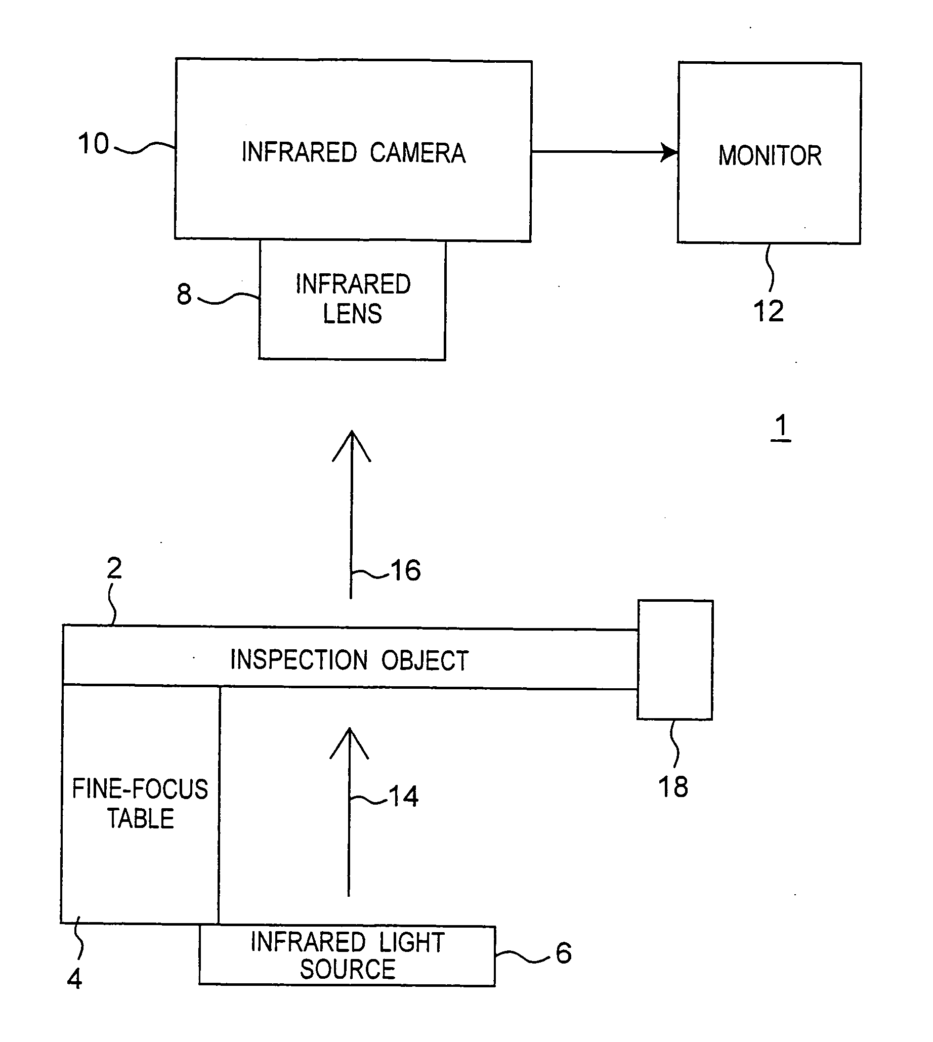
[0016]FIG. 1 is a block diagram showing a constitution of a semiconductor wafer inspection apparatus 1 according to first embodiment of the present invention. According to the semiconductor wafer inspection apparatus 1 in the first embodiment, a polycrystalline silicon substrate can be used as an inspection object 2, for example. The inspection object 2 is supported by a fine-focus table 4 and its horizontal and vertical positions can be determined by it. An infrared light source 6 is a light source to irradiate the inspection object 2 with infrared rays and may be a halogen lamp which can emit infrared rays, for example. A filter which can cut a visible light may be provided in front of the infrared light source 6 in order to make an image on a monitor 12 that will be described below clear. An infrared camera 10 including an infrared lens 8 collects the infrared rays from the inspection object 2 and converts the infrared rays to an electric signal and transmits th...

second embodiment

(Second Embodiment)

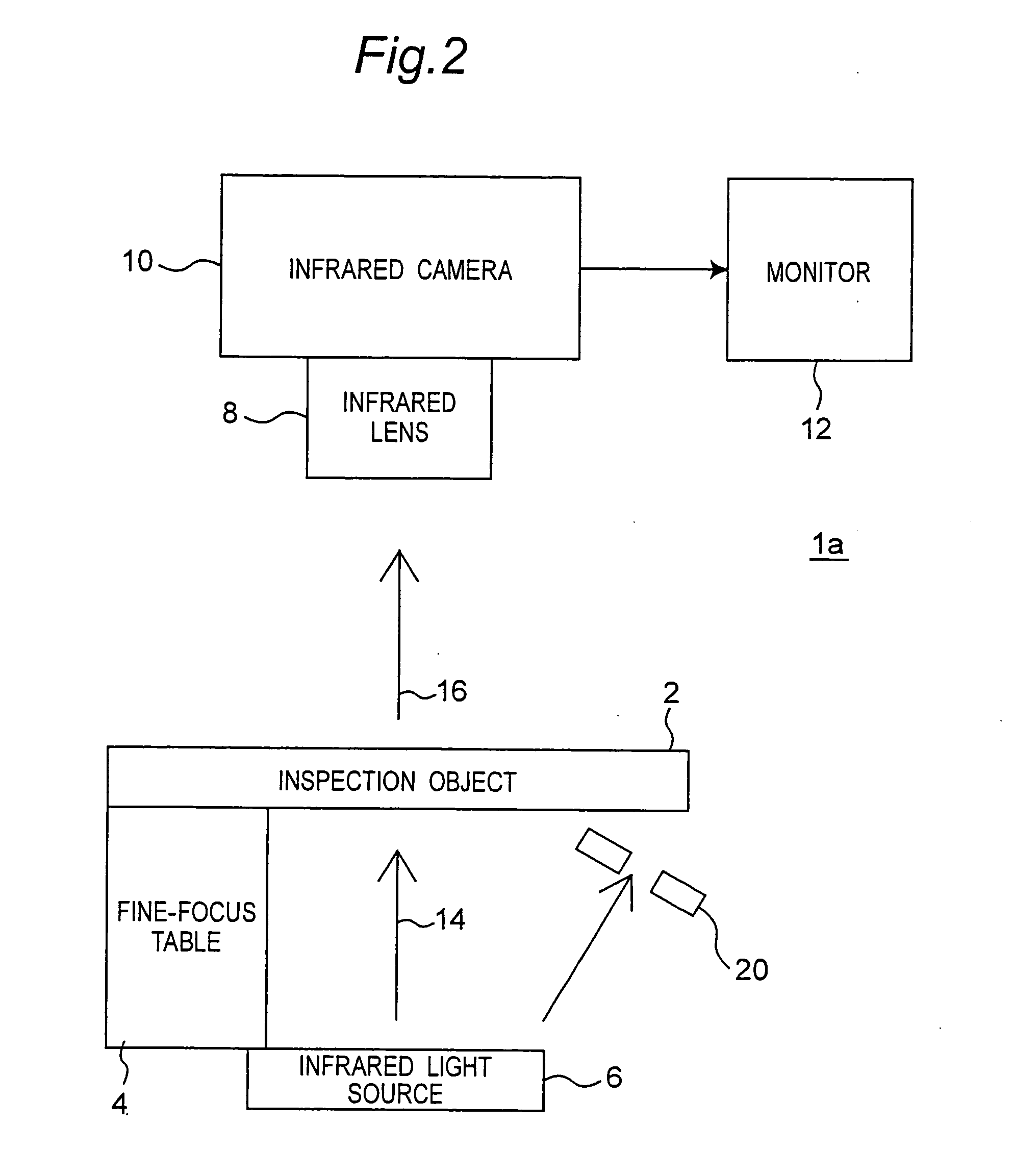
[0025]FIG. 2 is a block diagram showing a constitution of a semiconductor wafer inspection apparatus 1a according to second embodiment of the present invention. The semiconductor wafer inspection apparatus 1a is different from the semiconductor wafer inspection apparatus 1 according to the first embodiment in that a slit 20 is provided on a light path between an infrared light source and an periphery of a semiconductor wafer instead of the guide provided on the periphery of the semiconductor wafer as the infrared ray leakage preventing member. In addition, the same reference numerals are allotted to the same component substantially and their descriptions will be omitted.

[0026] As shown in FIG. 2, according to the second embodiment, when an end part of an inspection object 2 is observed, infrared rays 14 is applied from the infrared light source through the slit 20. The slit 20 blocks off a light path between the infrared light source 6 and a periphery of the insp...

third embodiment

(Third Embodiment)

[0029] Third embodiment is shown when the semiconductor wafer inspection apparatus shown in the first embodiment is used in a manufacturing process of a semiconductor wafer.

[0030] A semiconductor wafer having a defect part such as a crack and a semiconductor wafer having no defect can be discriminated by the inspection apparatus and the inspecting method shown in the first embodiment.

[0031] When the semiconductor wafer having the defect part such as the crack is put in a semiconductor wafer manufacturing equipment, the crack part is enlarged due to transportation or a heat treatment at the time of manufacturing steps, and the substrate is cracked into a plurality of parts in some cases. When the substrate is cracked, a defect of the equipment is generated and the equipment has to be stopped until the cracked substrate is removed, which causes manufacturing yield to be lowered and adversely affects an entire manufacturing line.

[0032] Therefore, when the semicondu...


PUM


Abstract

An infrared inspection apparatus includes: an infrared light source operable to irradiate an inspection object with infrared rays; an infrared lens operable to collect infrared rays which have passed through the inspection object; an infrared camera operable to receive the infrared rays collected by the infrared lens and to convert the infrared rays received into an electric signal to be output; a monitor operable to receive the electric signal from the infrared camera and to convert the electric signal into an image signal and to display an image based on the image signal; and an infrared ray leakage preventing member in at least one of a light path between the infrared light source and a periphery of the inspection object and a light path between the periphery of the inspection object and the infrared lens to prevent infrared rays from the infrared light source from reaching the infrared lens without passing through the inspection object.

Description

[0001] This application is based on Japanese Patent Application No. 2005-173423 filed in Japan on Jun. 14, 2005, the contents of which are hereby incorporated by reference. BACKGROUND OF THE INVENTION [0002] 1. Field of the Invention [0003] The present invention relates to an infrared inspection apparatus which irradiates an inspection object with infrared rays and observes the infrared rays that passed through the inspection object to inspect the inspection object, and more particularly to an infrared inspection apparatus for a semiconductor wafer in which a semiconductor wafer is used as the inspection object. [0004] 2. Description of the Related Art [0005] Conventionally, a semiconductor wafer inspection apparatus which detects a fine crack of a semiconductor wafer by irradiating the semiconductor wafer as the inspection object with infrared rays and observing the transmitted or reflected infrared rays has been developed. The Japanese Patent Laid-open Publication No.6-308042 disc...

Claims


Application Information

Patent Timeline
IPC IPC(8): G01N21/59G01N21/956H01L21/66
CPCG01N21/59G01N21/9505G01N21/9501
Inventor MATSUMOTO, NORIHISAMATSUNO, SHIGERU
Owner MITSUBISHI ELECTRIC CORP
Why Eureka
Try Eureka