LED package, manufacturing method thereof, and LED array module using the same

a technology of led array module and manufacturing method, which is applied in the direction of lighting support device, semiconductor/solid-state device details, lighting and heating apparatus, etc., can solve the problems of exponential decay of led performance, relatively long heat transfer path, and high power consumption of leds used in backlight units for lcds or lighting apparatuses. , to achieve the effect of high power led, excellent heat dissipation performance and low cos

Inactive Publication Date: 2006-12-14
SAMSUNG ELECTRONICS CO LTD
View PDF4 Cites 50 Cited by
  • Summary
  • Abstract
  • Description
  • Claims
  • Application Information

AI Technical Summary

Benefits of technology

[0014] Accordingly, it is one object of the present invention to provide a high power LED package with excellent heat dissipation performance, which can be manufactured at a low cost, and a manufacturing method thereof.

Problems solved by technology

LEDs used in backlight units for LCDs or in lighting apparatuses require high power consumption.
However, when the temperature rises, the performance of LEDs exponentially decays.
However, conventional LED packages, such as illustrated in FIG. 1, have relatively long heat transfer paths (e.g. LED-insulation layer-heat spreading member-solder-substrate).
As a result, conventional LED packages exhibit low heat dissipation performance due to an increase in thermal resistance, and thus are not suitable for high power LED packages.
When heat dissipation performance of an LED package is low, the LED lifespan is reduced, and peripheral components may deteriorate and become thermally deformed due to the high temperature, which may cause fatal damages to the system.
Additionally, conventional LED packages require many connections by wire bonding process.
When an LED array module is formed by using such conventional LED packages, the number of assembly processes required, including a process for soldering the plurality of packages on the substrate, is large, and thus the production cost is high.

Method used


Image

  • LED package, manufacturing method thereof, and LED array module using the same
  • LED package, manufacturing method thereof, and LED array module using the same
  • LED package, manufacturing method thereof, and LED array module using the same

Examples


Embodiment Construction

[0048] An LED package, a manufacturing method thereof and an LED array module using the same in accordance with exemplary embodiments of the present invention will now be described in detail with reference to the accompanying drawings. Well-known functions or constructions are not described in detail since they would obscure the invention in unnecessary detail.

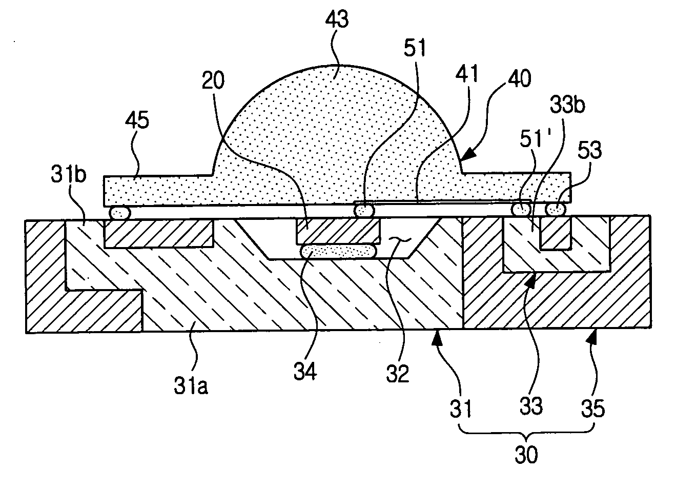
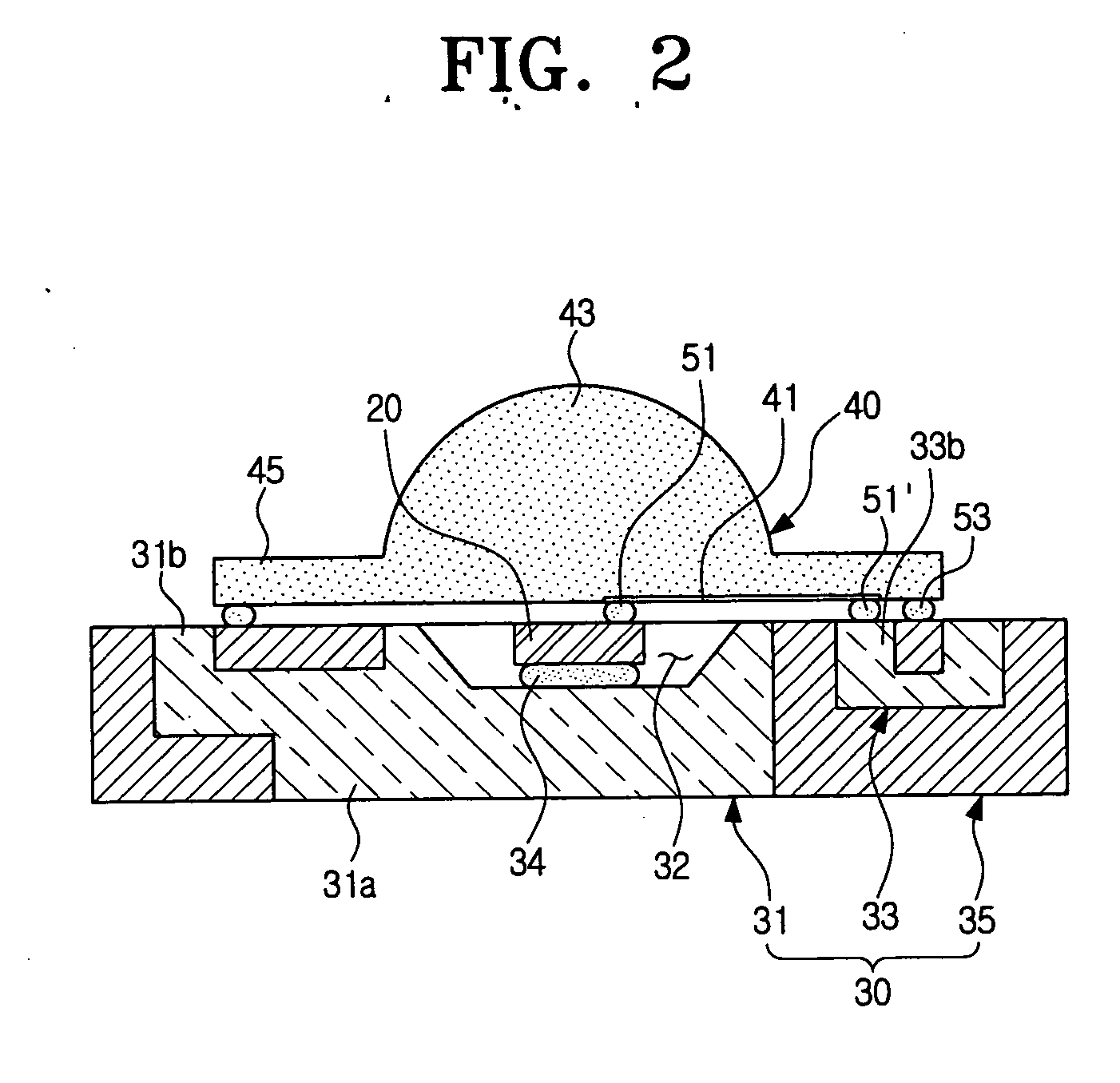
[0049] As illustrated in FIGS. 2 and 3, in accordance with one embodiment of the present invention, an LED package includes an LED 20, a substrate 30 on which the LED 20 is mounted, and a cap 40 for sealing up and electrically connecting the LED 20.

[0050] The substrate 30 includes at least two first and second conductor units 31 and 33, and a non-conductor unit 35 for electrically insulating the conductor units 31 and 33. The first conductor unit 31 includes a heat dissipation unit 31 a used as a heat transfer path of the LED 20, and a first electrode unit 31b for power supply. The second conductor unit 33 includes a second ...


PUM

PropertyMeasurementUnit
conductiveaaaaaaaaaa
depthaaaaaaaaaa
non-conductoraaaaaaaaaa

Abstract

An LED package includes a substrate, an LED, and a cap. The substrate includes a first conductor unit, a second conductor unit, and a non-conductor unit which electrically insulates the first and second conductor unit. The LED is bonded to the first conductor unit. The cap is mounted on the substrate over the LED and comprises a conductive wire which connects the LED to the second conductor unit.

Description

CROSS-REFERENCE TO RELATED PATENT APPLICATIONS [0001] This application claims priority under 35 U.S.C. § 119 from Korean Patent Application No. 2005-49896, filed on Jun. 10, 2005, the entire content of which is incorporated herein by reference.BACKGROUND OF THE INVENTION [0002] 1. Field of the Invention [0003] Methods and apparatuses consistent with the present invention relate to a light emitting diode (LED) package that can be used as a backlight unit of an LCD and a lighting apparatus, a manufacturing method thereof, and an LED array module using the same. [0004] 2. Description of the Related Art [0005] LEDs are popular in the fields of advertising and electronics due to their long lifespan and low power consumption. There have also been attempts to use LEDs in backlight units of LCDs. It is also expected that LEDs will be used in indoor or outdoor lighting apparatuses in the near future. As the application range of LEDs is expanded, there are increasing demands for LED packages ...

Claims


Application Information

Patent Timeline
Patent Type & Authority Applications(United States)
IPC IPC(8): F21V5/04H01L33/00H01S4/00H01L33/60H01L33/62H01L33/58H01L33/64
CPCH01L33/58H01L33/62H01L33/647H01L2224/48091H01L2224/73265H01L2924/01078Y10T29/49002H01L2924/15153H01L2924/15165H01L2924/01079H01L2924/12041H01L2924/01019H01L2924/00014
Inventor SHIN, KYU-HOSHIN, SU-HOKWEON, SOON-CHEOLMOON, CHANG-YOULCHOI, JIN-SEUNG
Owner SAMSUNG ELECTRONICS CO LTD
Why Eureka
Try Eureka