Storage device and semiconductor apparatus

a storage device and semiconductor technology, applied in the field of storage devices and semiconductor devices, can solve the problems of slow reading speed of ferams, limited number of rewritable times, and difficulty in non-destructive reading by ferams, and achieve the effect of reducing the period of time necessary for recording information and stable recording

Inactive Publication Date: 2006-12-14
SONY CORP
View PDF4 Cites 19 Cited by
  • Summary
  • Abstract
  • Description
  • Claims
  • Application Information

AI Technical Summary

Benefits of technology

[0041] In the storage device and the semiconductor apparatus, information can be stably recorded, the period of time necessary for recording information can be reduced, and writing and erasing can be performed.

Problems solved by technology

However, since DRAMs are volatile memories, which lose information when the power is turned off, nonvolatile memories, which hold information even after the power is turned off, are desired.
However, under the present situation, it is difficult for FeRAMs to perform nondestructive reading.
Since FeRAMs perform destructive reading, the reading speed of FeRAMs is slow.
In addition, since there is a restriction on the number of times polarization reversal according to reading or recording can be performed, the number of rewritable times is limited.
Thus, a large amount of current is necessary for recording.
Thus, phase change memories are susceptible to changes in the ambient temperature.
Thus, processing at a temperature of about 600° C. is necessary, it is extremely difficult to manufacture monocrystal of the suggested material, and miniaturization is difficult due to the influence of grain boundary when polycrystal is used.
Thus, a pulse voltage with a pulse width shorter than about 100 nanoseconds has a lower resistance ratio by recording and is susceptible to variations in the resistance after recording.
Thus, it is difficult to perform stable recording.
Thus, a longer period of time is spent for recording, and, for example, it is difficult to perform overwriting of data or the like at high speed.

Method used


Image

  • Storage device and semiconductor apparatus
  • Storage device and semiconductor apparatus
  • Storage device and semiconductor apparatus

Examples


Embodiment Construction

[0054] Embodiments of the present invention will be described with reference to the drawings.

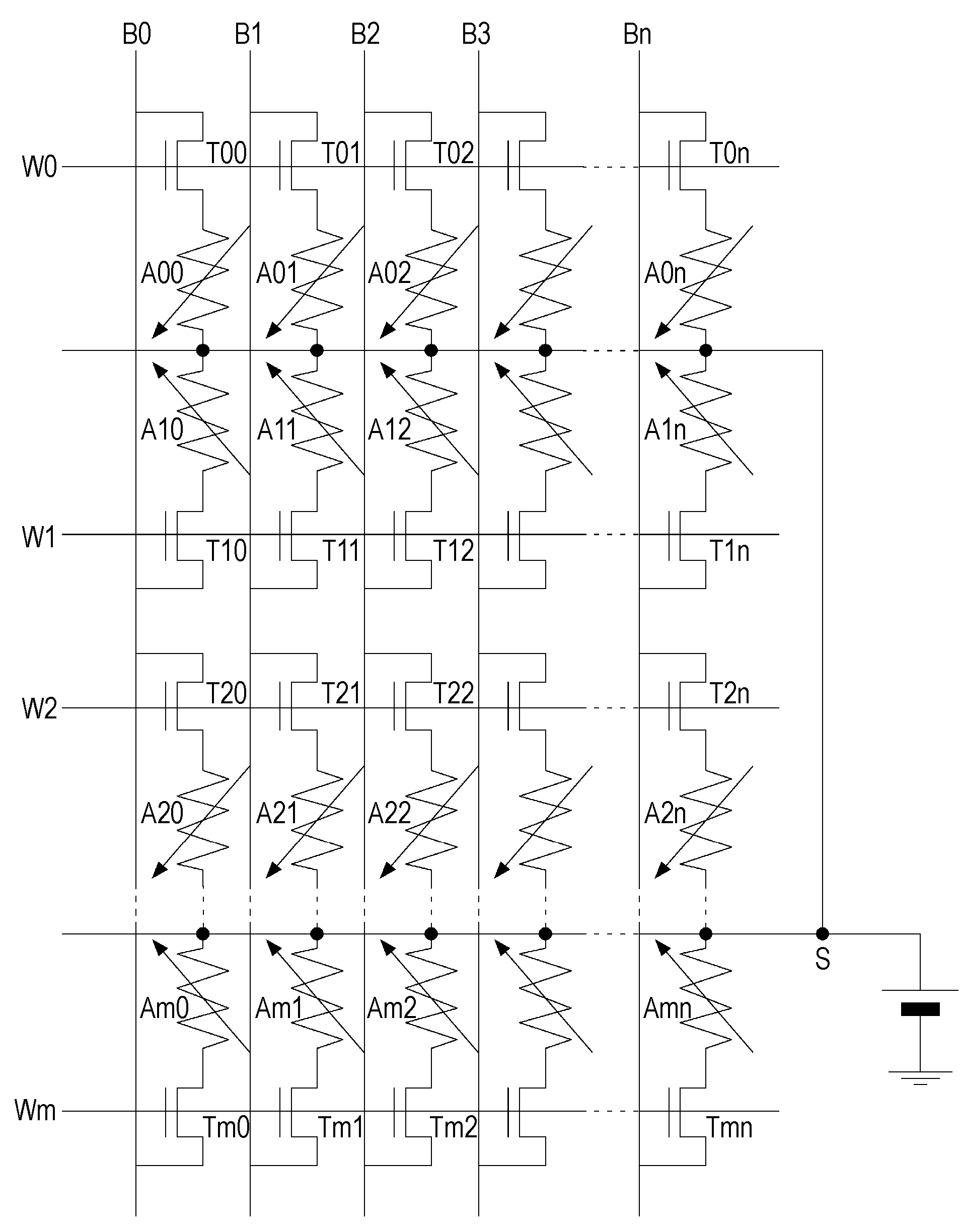
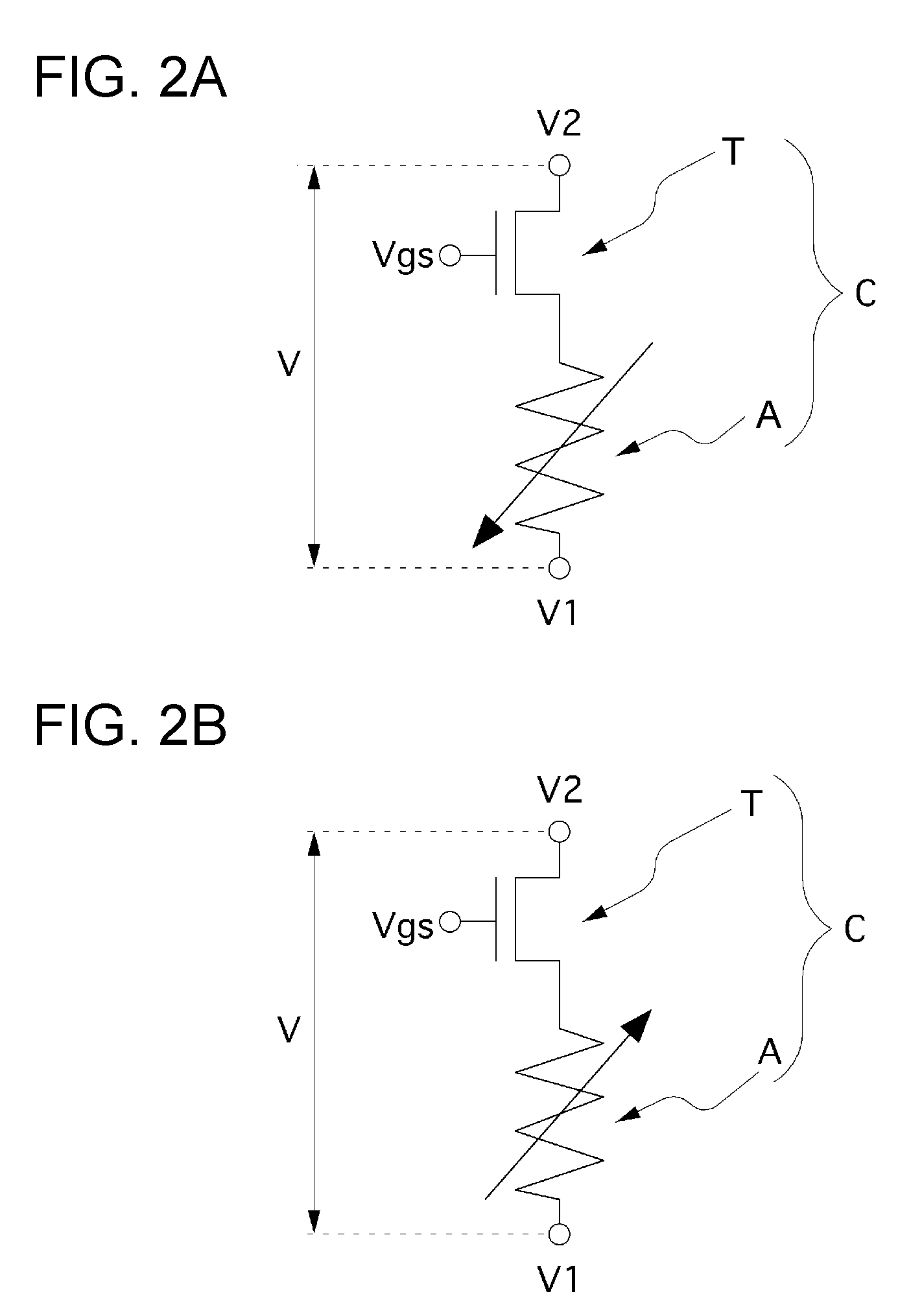
[0055] In the embodiments of the present invention, a storage device includes a resistance change storage element (hereinafter, referred to as a memory element) used for a memory cell.

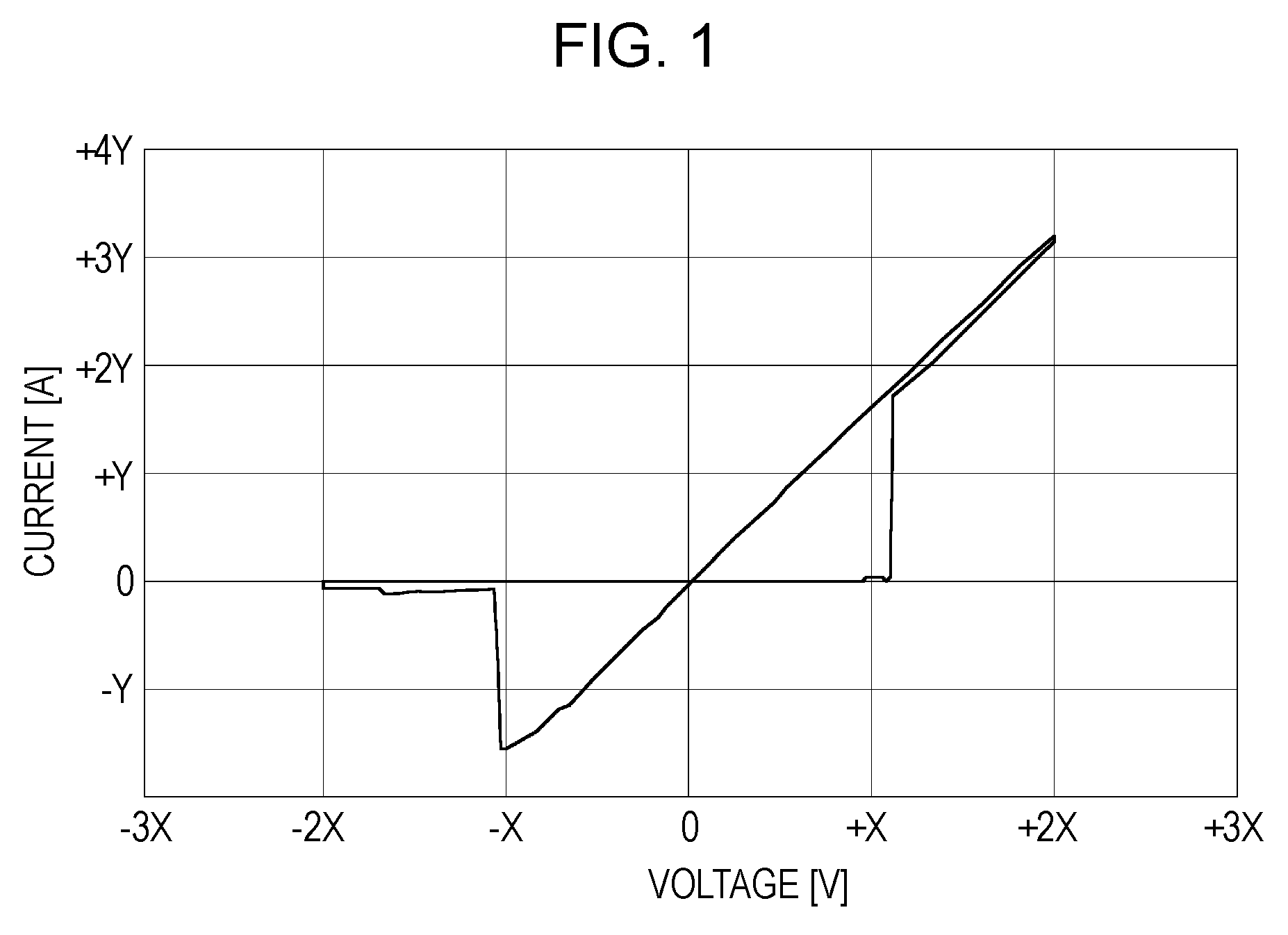
[0056]FIG. 1 is a graph showing a current-voltage (I-V) change of a memory element used in a storage device according to an embodiment of the present invention.

[0057] As a memory element having the I-V characteristic shown in FIG. 1, for example, a storage element including a storage layer that is sandwiched between a first electrode and a second electrode (for example, between a lower electrode and an upper electrode) and that is made of an amorphous thin film, such as a rare-earth oxide film or the like, is used.

[0058] In the initial state, the memory element has a high resistance (for example, 1 MΩ or more), and a current does not flow easily. Referring to FIG. 1, when a voltage of +1.1× V (for example, ...


PUM


Abstract

A storage device includes a storage element having first and second terminals that cause a first electrical characteristic change when an electric signal of a first threshold level or higher is applied and that cause a second electrical characteristic change, which is asymmetrical to the first electrical characteristic change, when an electric signal of a second threshold level or higher, the polarity of the electric signal of the second threshold level or higher being different from the polarity of the electric signal of the first threshold level or higher, is applied; and a unipolar transistor connected in series with the storage element. One of the first terminal and the second terminal of the storage element is electrically connected to the unipolar transistor. The unipolar transistor has a negative polarity or a positive polarity in accordance with the first terminal or the second terminal electrically connected to the unipolar transistor.

Description

CROSS REFERENCES TO RELATED APPLICATIONS [0001] The present invention contains subject matter related to Japanese Patent Application JP 2005-169035 filed in the Japanese Patent Office on Jun. 9, 2005, the entire contents of which are incorporated herein by reference. BACKGROUND OF THE INVENTION [0002] 1. Field of the Invention [0003] The present invention relates to storage devices and semiconductor apparatuses, and more particularly, to a storage device and a semiconductor apparatus that include memory cells each including a storage element storing and holding information in accordance with an electric resistance state. [0004] 2. Description of the Related Art [0005] In information apparatuses, such as computers, high-density dynamic random access memories (DRAMs) with high operation speed are widely used as random access memories (RAMs). [0006] However, since DRAMs are volatile memories, which lose information when the power is turned off, nonvolatile memories, which hold informat...

Claims


Application Information

Patent Timeline
Patent Type & Authority Applications(United States)
IPC IPC(8): G11C11/00
CPCG11C13/0007G11C13/003G11C13/0069G11C2013/0078G11C13/0004G11C2213/34G11C2213/76G11C2213/79G11C2213/15G11C11/21
Inventor HACHINO, HIDENARIOKAZAKI, NOBUMICHIARATANI, KATSUHISA
Owner SONY CORP
Why Eureka
Try Eureka