Light emitting device and electronic device

a technology of light emitting devices and electronic devices, which is applied in the direction of solid-state devices, semiconductor devices, organic semiconductor devices, etc., can solve the problems of reducing efficiency and low efficiency of color conversion methods, and achieves the effects of reducing driving voltage, operating more efficiently, and operating more efficiently

Inactive Publication Date: 2006-12-21
SEMICON ENERGY LAB CO LTD
View PDF36 Cites 83 Cited by
  • Summary
  • Abstract
  • Description
  • Claims
  • Application Information

AI Technical Summary

Benefits of technology

[0024] By the invention, a light emitting device which uses a color conversion layer can operate more efficiently. Mor...

Problems solved by technology

However, the efficiency of the color conversion method is still low as compared to the separate deposition method in which three colors are directly emitted from respective light emitting el...

Method used


Image

  • Light emitting device and electronic device
  • Light emitting device and electronic device
  • Light emitting device and electronic device

Examples


embodiment mode 1

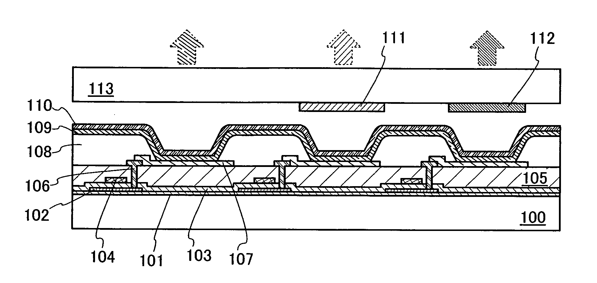
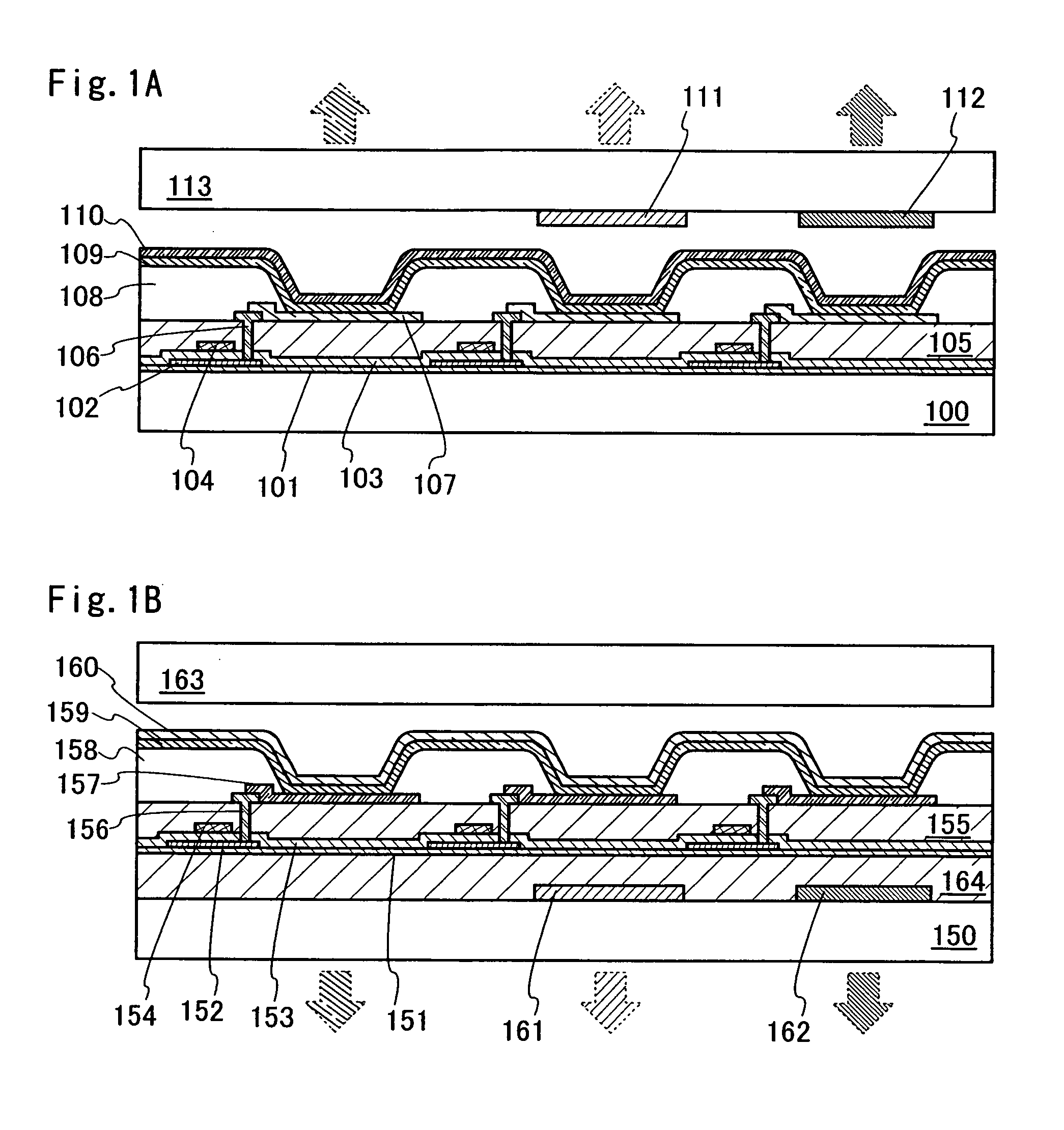
[0046]FIG. 1A shows an example of a structure of a light emitting device of the invention. FIG. 1A is a portion of a cross sectional view showing a pixel portion of an active matrix light emitting device. The light emitting device of the invention shown in FIG. 1A includes a substrate 100, a base insulating film 101, a semiconductor layer 102, a gate insulating film 103, a gate electrode 104, an interlayer insulating film 105, a connecting portion 106, a first electrode 107 of a light emitting element, a partition 108, a layer 109 containing an organic compound, a second electrode 110 of the light emitting element, a color conversion layer (green) 111, a color conversion layer (red) 112, and a counter substrate 113. It is to be noted that a sealing material is omitted in FIGS. 1A and 1B.

[0047] The light emitting element is formed in a portion where the layer 109 containing an organic compound is sandwiched between the first electrode 107 and the second electrode 110 of the light em...

embodiment mode 2

[0096]FIG. 1B is a view showing a light emitting device of the invention with a different structure from FIG. 1A. The light emitting device of the invention shown in FIG. 1B includes a substrate 150, a base insulating film 151, a semiconductor layer 152, a gate insulating film 153, a gate electrode 154, an interlayer insulating film 155, a connecting portion 156, a first electrode 157 of a light emitting element, a partition 158, a layer 159 containing an organic compound, a second electrode 160 of the light emitting element, a color conversion layer (green) 161, a color conversion layer (red) 162, a counter substrate 163, and a depression / projection smoothing layer 164. In this embodiment mode, a bottom emission type light emitting device in which the light emitting element emits light to the first electrode 157 side is shown as an example. In this embodiment mode, the first electrode 157 is formed of a light-transmissive conductive material in order to extract light from the first...

embodiment mode 3

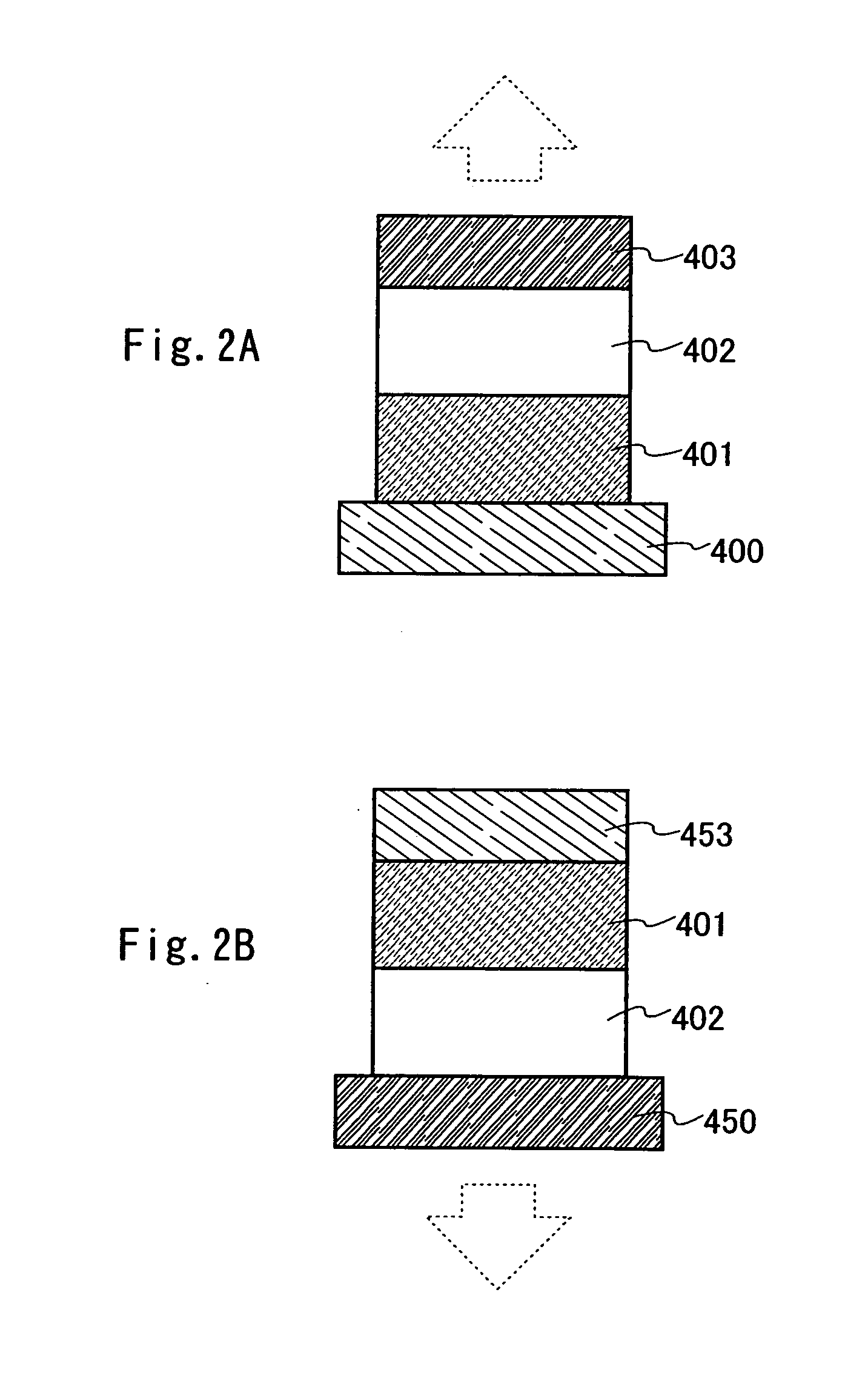
[0100]FIG. 4A is a view showing a light emitting device of the invention with a different structure from FIG. 1A. The structure of this embodiment mode is almost the same as the structure described in Embodiment Mode 1, besides a blue color filter 115 is provided. When light is emitted from a light emitting layer through a blue color filter, color purity can be improved. This is a favorable structure with relatively less loss of light since the light emitted from the light emitting element has a wavelength in a region near a blue color. It is also a favorable structure that the light emitted from the light emitting element is adjusted to the absorption of the color conversion layer (green) 111 and the color conversion layer (red) 112 and color purity of blue color is improved with a color filter. It is to be noted in FIG. 4A that a sealing material is not shown.

[0101] The color filter 115 may be a color conversion layer (blue) for converting light of a near-ultraviolet region to a ...


PUM


Abstract

The invention provides a light emitting device which uses a color conversion layer, with high light emission efficiency and a low driving voltage. The light emitting device includes a light emitting element having a pair of electrodes and a layer containing an organic compound sandwiched between the pair of electrodes, and a color conversion layer which absorbs light emitted from the light emitting element and emits light with a longer wavelength than a wavelength of the absorbed light. A portion of the layer containing an organic compound includes a buffer layer containing a composite material including an organic compound having a hole transporting property and a metal compound. The thickness of the buffer layer is determined so that the light emission efficiency becomes high.

Description

BACKGROUND OF THE INVENTION [0001] 1. Field of the Invention [0002] The present invention relates to a light emitting device using a light emitting element which emits light when a current is supplied. In particular, the invention relates to a light emitting device which has a light emitting element having a layer containing an organic material and which realizes full color display by using a color conversion layer. [0003] 2. Description of the Related Art [0004] Development has been made on a light emitting device which has a layer containing an organic material sandwiched between a pair of electrodes and has a light emitting element which emits light when a current is supplied between the electrodes. Such a light emitting device is advantageous in realizing thinness and lightweight as compared to other display devices which are called thin display devices. In addition, being self-luminous type, such a light emitting device has favorable visibility and fast response speed. Moreover...

Claims


Application Information

Patent Timeline
IPC IPC(8): H01L33/00
CPCH01L27/322H01L27/3244H01L29/78645H01L51/50H01L27/1288H01L51/5265H01L2251/5323H01L2251/558H01L51/5262H10K59/38H10K59/12H10K50/00H10K50/85H10K50/852H10K2102/3031H10K2102/351
Inventor YAMAZAKI, SHUNPEIMATSUBARA, TOMOE
Owner SEMICON ENERGY LAB CO LTD
Why Eureka
Try Eureka